| ID |
Date |
Author |
Project |
Subject |
Run Number |
Events |
StartTime |
EndTime |
|
59
|
Tue Jun 3 12:41:22 2008 |
Eudet Telescope | | useful eudaq software commands | (work in progress) | | | | to show information about a run (number of events, start and end timestamp,....:
./TestReader.exe -b -e 2828 |
|
57
|
Tue Jun 3 11:03:27 2008 |
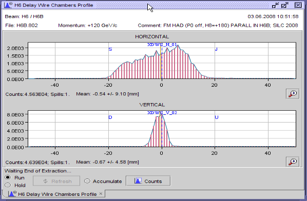
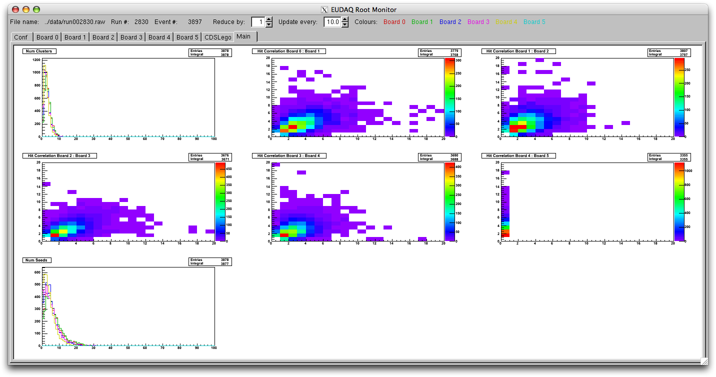
Thomas Bergauer | | telescope alignment run | run2830 | 3897 | 2008-06-03 10:52:16.783 | 2008-06-03 10:58:52.790 | | telescope run with reduced beam intensity (BEND4=-600A instead of -620A and BEND7=-605A instead of -615A) |
| Attachment 1: beam_profile_with_modified_BEND4and7.png
|  |
| Attachment 2: hit_correlations.png
|  |
|
29
|
Sun Jun 1 17:01:12 2008 |
Thomas Bergauer | SiLC | path do data | | | | | The data of all runs are stored on eudetmac001.cern.ch:
APVDAQ: /Volumes/Data/eudet/APVDAQ/silc/data
Telescope data: /Volumes/Data/eudet/Data/testing
all data will be saved to an external Firewire disk (Vienna Backup) and to CASTOR |
|
15
|
Sat May 31 13:34:28 2008 |
Thomas Bergauer | | how to copy data from lab2pc to eudetmac | | | | | rsync -rltvz --exclude "data_vie" --exclude "hitfit_cern08" --exclude "output_vie" --exclude "run2719*" --rsh="ssh -C -p222" friedl@routerhephy.cern.ch:/cygdrive/f/testbeam/cern_jun08/ /Volumes/Data/eudet/APVDAQ/
but replace run2719 with the name of the run file currently active (data taking)
and use Markus' password |
|
67
|
Wed Jun 4 15:41:04 2008 |
Thomas Bergauer | | end. | | | | | | testbeam is over. DUTs and APVDAQ have been dismounted and will be shipped back to Vienna. EUDET telescope is still in H6B and taking data for alignment and pedestal during the night. |
|
6
|
Wed May 14 09:21:39 2008 |
stephan h�nsel | SiLC | capacity measurements - HPK-ILC-TS-6687-24 | | | | | ich hab mal die Kapazit�ts-Messungen vom Thomas in ein Diagram gegeben
interessant ist, dass die Kapazit�t mit 2 intermediate strips (int. strips) kleiner ist als mit einem int. strip -> das bedeutet, dass der eine int. strip breiter ist als die 2 int. strips zusammen - oder?
weiters d�rfte die breite des einen int. strips mit der stripwith leicht variieren
(zur Erinnerung: Plattenkondensator - C = e eo A / d ) |
| Attachment 1: capacity-TS24.eps
|
| Attachment 2: capacity_measurements_ACTS-24.opj
|
|
19
|
Sat May 31 18:33:50 2008 |
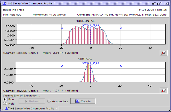
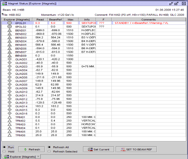
Thomas Bergauer | other | beam profile | | | | | Beam configuration
Beam configuration file: H6b.802 (FM HAD (P0 off, H8=+180) PARLALLEL IN H6B SILC 2008
Rate: 5.7E5 particles/spill (measured with SCINT8 in beamline)
Particle Production Applet
Calculator applet
For +120 Gev/c beam:
|
Pi+ | 55.67 %
| |
p | 38.95 %
| |
K+ | 5.38 %
|
|
| Attachment 1: Picture_1.png
|  |
| Attachment 2: beamline_settings.png
|  |
|
30
|
Sun Jun 1 18:23:38 2008 |
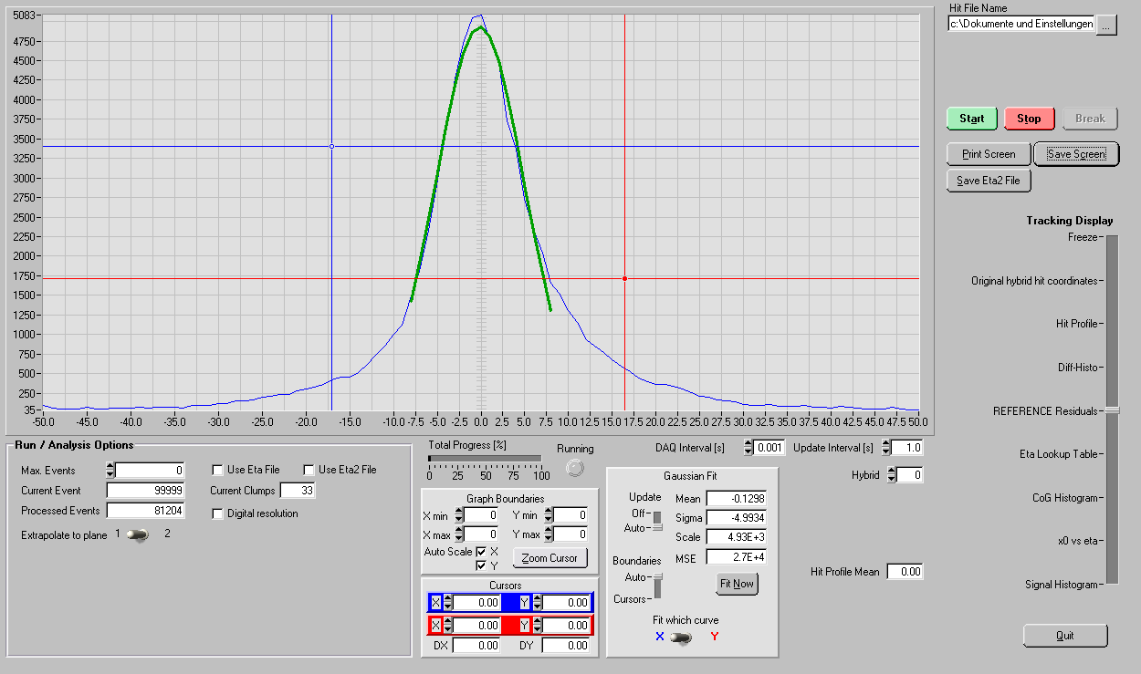
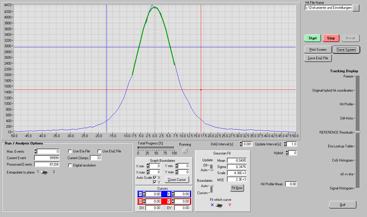
Markus Friedl | SiLC | Very simple tracking | run2719 | 100000 | | | Very simple alignment (manual linear x direction shifting only, no rotation, assuming equal z spacing) and tracking.
Reference plane = Module 3 (~center)
Deviation calculated from track prediction using the other layers.
Simple Center-of-gravity algorithm (as of APVDAQ_Analysis), no eta applied.
Using only events which have exactly 1 hit per plane (~80% of all events).
Results:
Residual RMS = 4.99 um (REFERENCE against neighbor layers 2+4 only)
Residual RMS = 6.35 um (REFERENCE against all 7 other layers) -> needs more sophisticated alignment |
| Attachment 1: silc_verysimple_res_2REF4.png
|  |
| Attachment 2: silc_verysimple_res_012REF4567.png
|  |
|
8
|
Mon May 19 15:14:40 2008 |
Markus Friedl | other | Tentative Beam Test Schedule | | | | | Wed 28 May: ~16:00 arrival, unpacking
Thu 29 May: installation
Fri 30 May: beam on
1) Telescope + 8xSilC (~7hrs, overnight; first part)
2) 8xSilc, no telescope (fast runs during day)
3) Telescope + 8xSilC (~7hrs, overnight; second part after DUT shift)
4) 1xSilc, rotation
5) Belle, telescope
* starting telescope alignement
* adc delay scan, intcal, pedrun, pedcorr
* DUT alignement
* std. settings, telescope zero supr.(zp) 1st half, lunch break
* std. settings, telescope zero supr. 2nd half
* std. settings, telescope raw data, 1st half
* std. settings, telescope raw data, 2nd half
* optionally HV scan, tel. zp., (10 HV settings --> 2x 10 runs)
* unmount 7 DUTs
* std run 0 deg., (2 runs)
* angle scan (about 10 runs)
* install Belle DUT
* std. settings, telescope raw, transparent mode
* std. settings, telescope sp, transparent mode, high statistics
* std. settings, telescope sp, processed mode, high statistics |
|
27
|
Sun Jun 1 15:52:03 2008 |
Eudet Telescope | SiLC | Telescope Pedestal Run | run2738 | 1247 | 1.6.2008. 15:50 | 1.6.2008. 15:58 | Telescope Pedestal Run
no DUTs!
no Beam!
Config File: test5boards.conf |
|
5
|
Fri May 9 15:29:28 2008 |
Thomas Bergauer | SiLC | Sensor Layout | | | | |
| |
pplus strip |
number of |
| |
width |
intermediate |
| strips |
[µm] |
strips |
| 16 |
6 |
no |
| 16 |
10 |
no |
| 16 |
12.5 |
no |
| 16 |
15 |
no |
| 16 |
20 |
no |
| 16 |
25 |
no |
| 16 |
6 |
single |
| 16 |
7.5 |
single |
| 16 |
10 |
single |
| 16 |
12.5 |
single |
| 16 |
15 |
single |
| 16 |
17.5 |
single |
| 16 |
6 |
double |
| 16 |
7.5 |
double |
| 16 |
10 |
double |
| 16 |
12.5 |
double |
Stephan: weil ichs immer hier suche hab ich das Wafer Layout file geadded ;-) |
| Attachment 1: test-AC-2.pdf
|
| Attachment 2: 070516-SiLC_WaferLayout.pdf
|
|
3
|
Wed May 7 16:28:23 2008 |
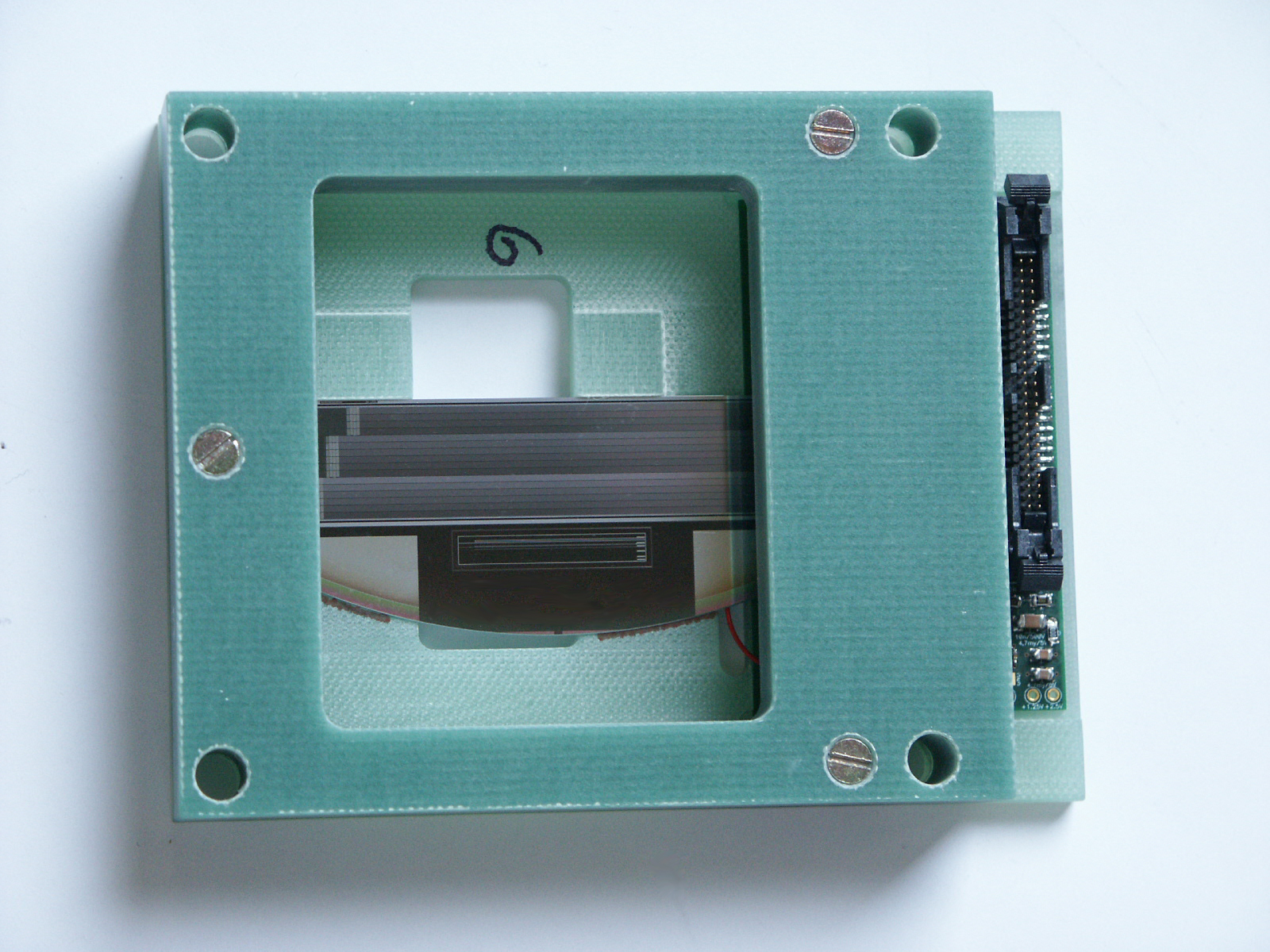
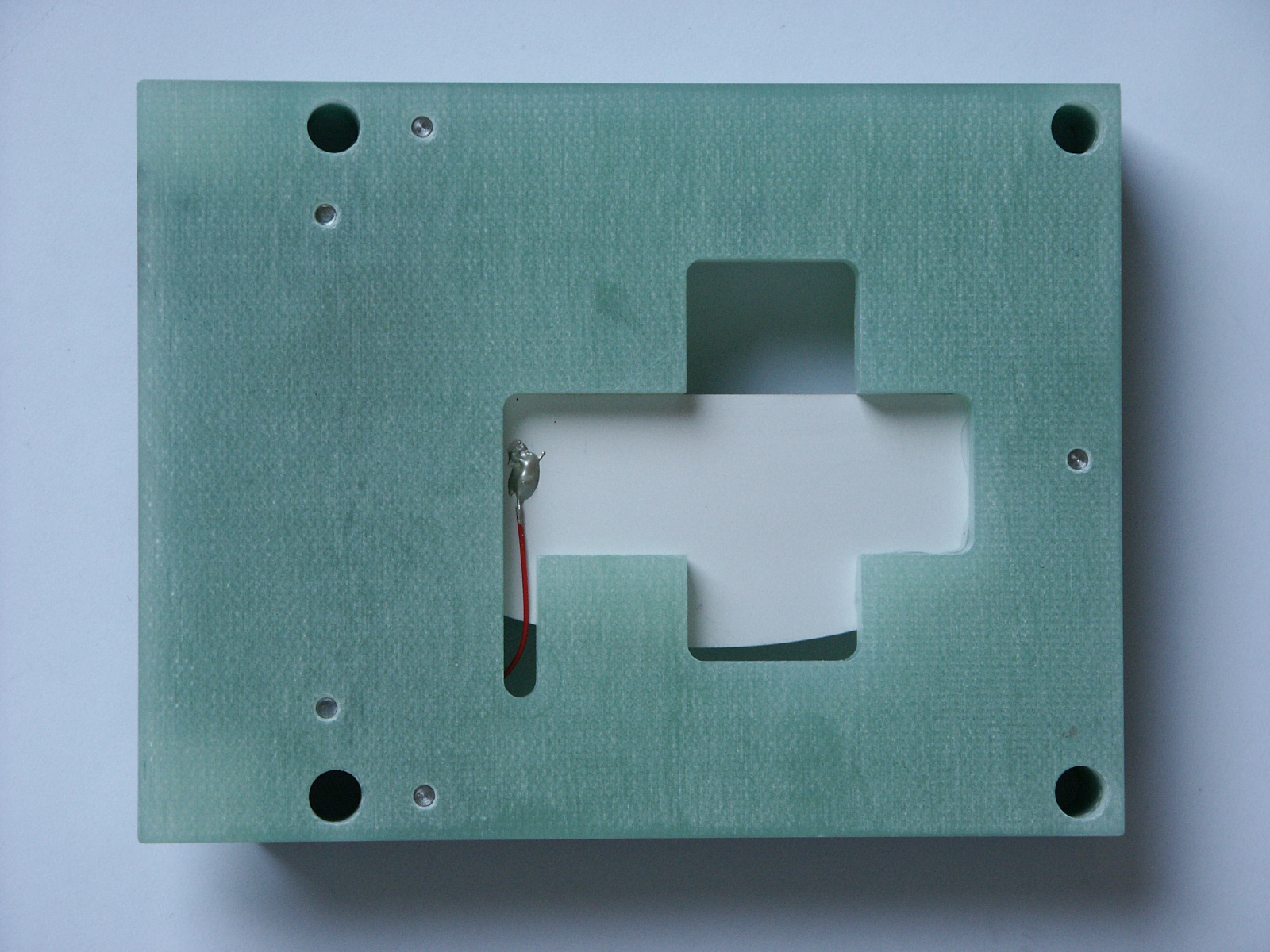
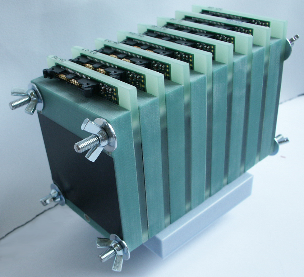
stephan h�nsel | SiLC | Photos | | | | | Module Photos
topview of module (without cover)
bottomview of module (without cover)
8 modules on table |
| Attachment 1: module-top.jpg
|  |
| Attachment 2: module-bottom.jpg
|  |
| Attachment 3: 8Modules.jpg
|  |
|
10
|
Fri May 23 15:17:49 2008 |
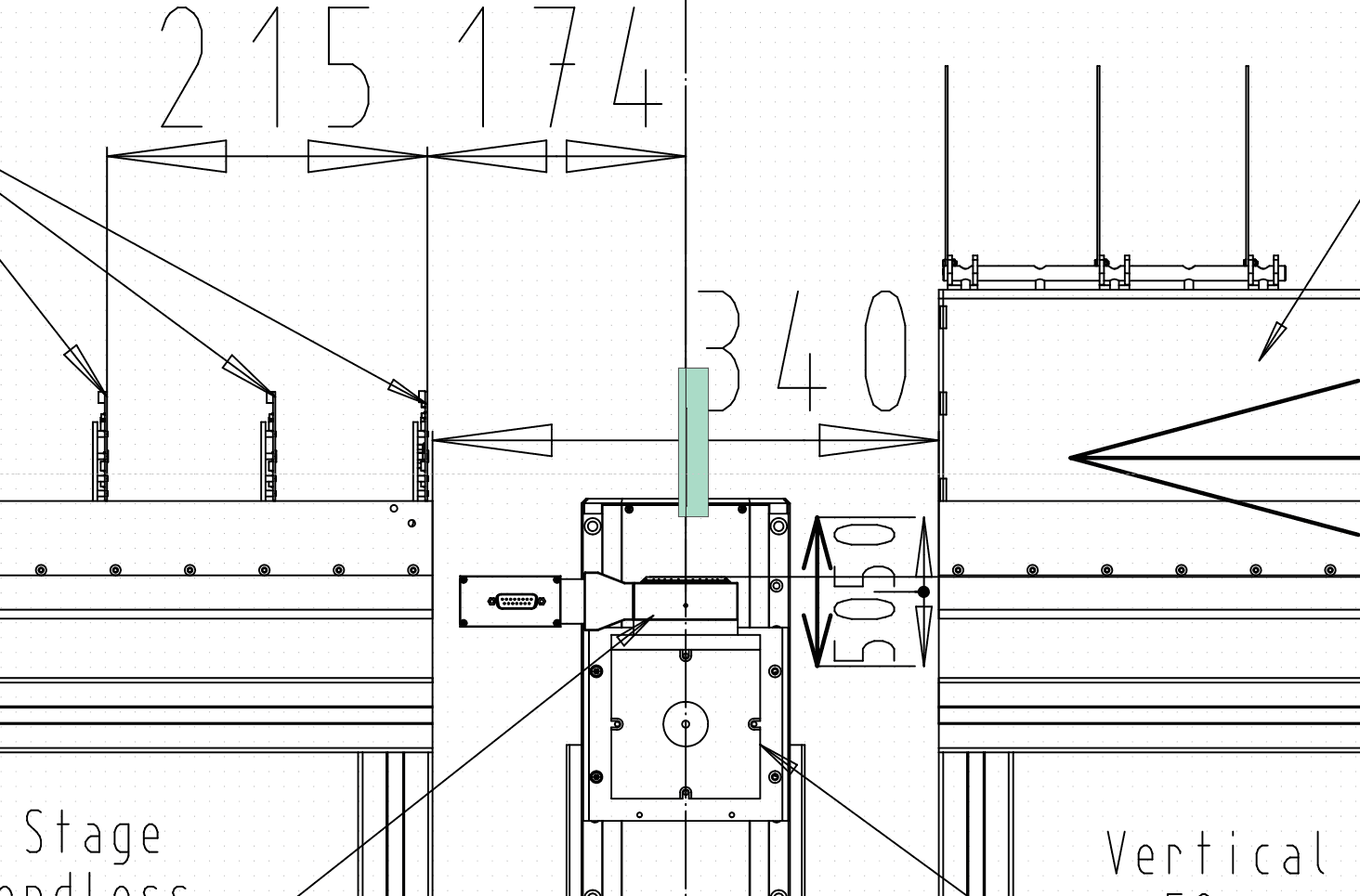
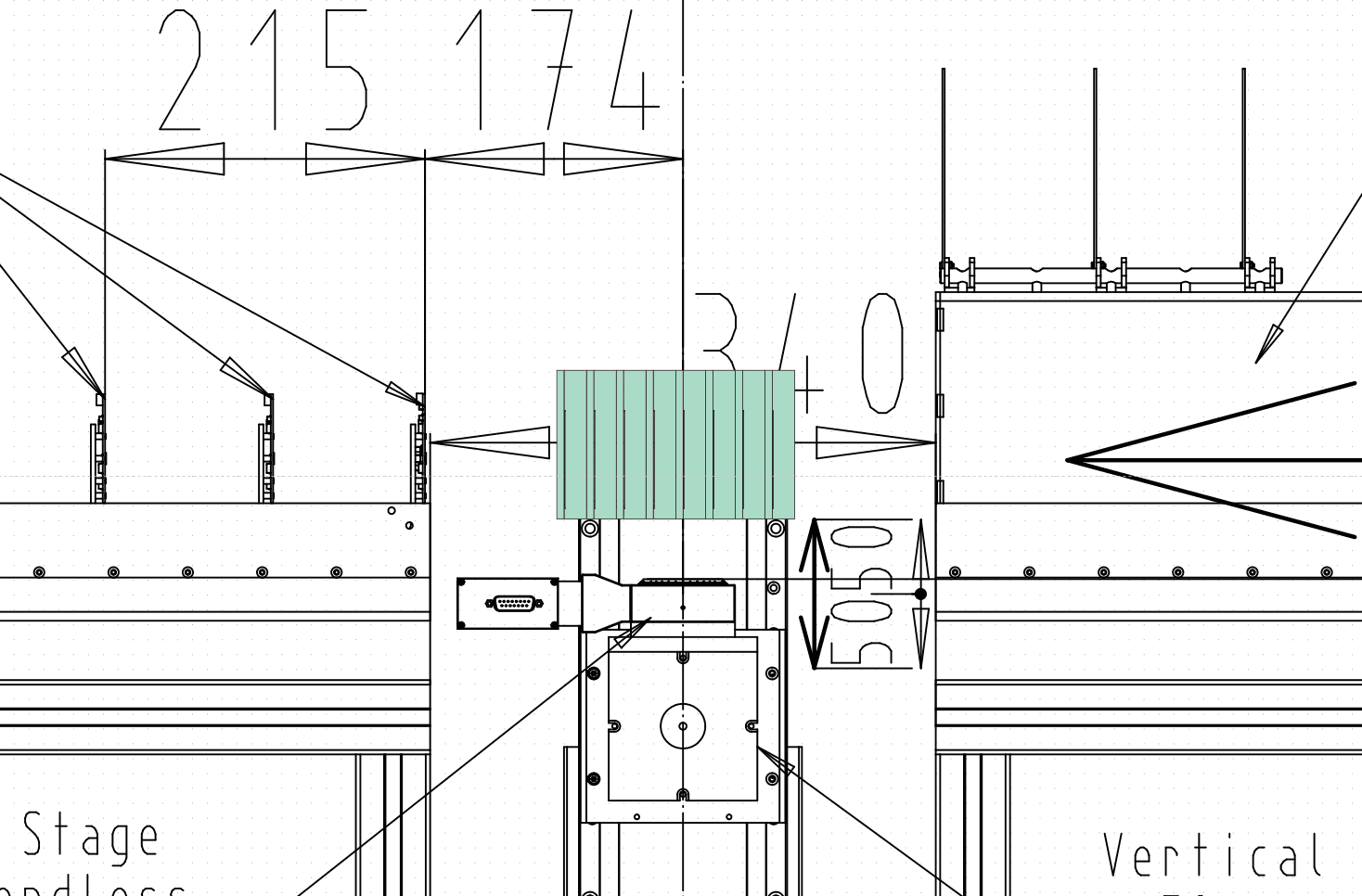
Markus Friedl | SiLC | Module/chip/strip/zone numbering scheme | (work in progress) | | | | The SILC DUT is a stack of 8 silicon sensors surrounded by the telescope.
The spacing between each of the 8 layers is 20mm. Seen with the beam, the fourth layer is exactly centered
between the telescope legs. This means that the stack as a whole is not exactly centered, as there is no
'center' module with an even number of layers. Please refer to drawings "telecope_single_dut.gif" and
"telescope_8_dut.gif" below.
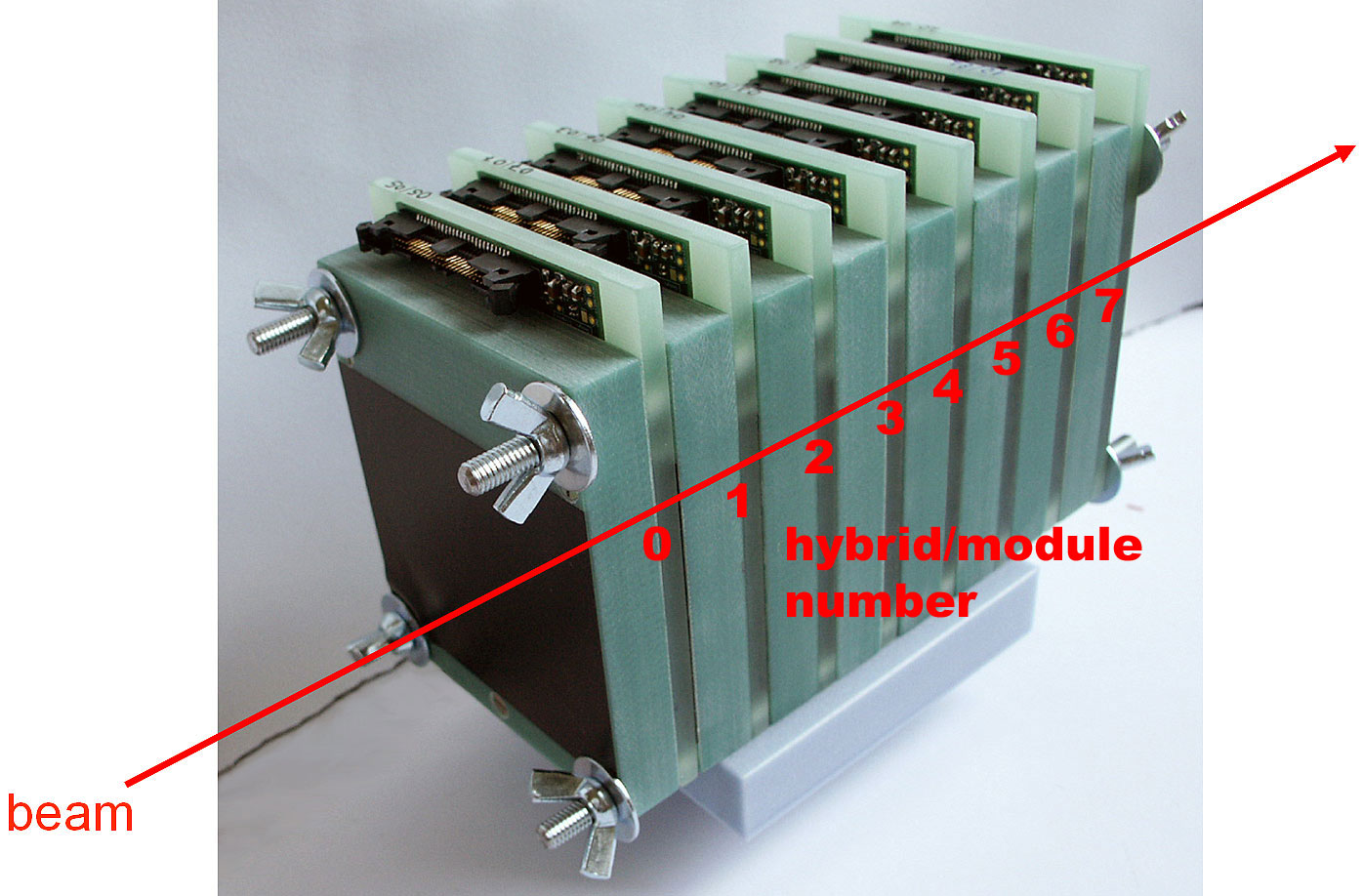
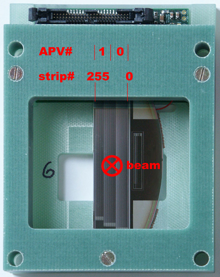
Each sensor has 256 strips, which are read out by 2 APV25 chips. The numbering order of the modules follows the
beam direction (see drawing "silc_dut_stack_beam.jpg"). Modules will have the connector (and thus APV25 hybrid)
at the top as shown in the photos. The numbering scheme within one module is shown in drawing
"silc_dut_beam.jpg": Looking with the beam, strips are numbered from right to left. The strip pitch is 50um
everywhere.
The APVDAQ software works on APV25 level for the data acquisition, where raw data is saved. In that case, the
APVs are consecutively numbered 0,1 (=module 0), 2,3 (=module 1), 4,5 (=module 2), ... ,14,15 (=module 7).
In later steps of the analysis, data are presented on a module [0..7] / strip [0..511] base.
Zone numbers were removed, now everything is zone=1.
(Zone 0 is a reserved value and hence the actual zone counting starts with 1.)
The 256 strips are divided into 16 groups of 16 strips each with different strip width and intermediate strips,
according to the table below:
pplus strip number of
width intermediate
group# strips [�m] strips
0 16 6 none
1 16 10 none
2 16 12.5 none
3 16 15 none
4 16 20 none
5 16 25 none
6 16 6 single
7 16 7.5 single
8 16 10 single
9 16 12.5 single
10 16 15 single
11 16 17.5 single
12 16 6 double
13 16 7.5 double
14 16 10 double
15 16 12.5 double
Please note that the strip pitch is 50�m everywhere, but between each group there is a gap of a single missing
strip. Hence, when calculating the coordinate from the strip number, one must take those distinctive gaps into
account.
We assume that we have a fractional strip position, where the fraction denotes (e.g.) the center of gravity of
the cluster. In order to convert this into a coordinate, we can use the following approach (where s is the
(fractional) strip number and x ist the fractional coordinate [�m]):
/* *** tested and works *** */
double strip2x(double strip)
{
unsigned short ints;
// this is the integral part of the strip number
ints = (unsigned short) strip;
return ( 50.0 * ( strip + ( ints >> 4 ) ) + ( ( (ints+1) & 15 ) ? 0.0 : ( strip - ints ) * 50.0 ) );
// pitch strip
// gaps between zones
// outside gap ? do nothing
// account for double pitch within gap
} |
| Attachment 1: telescope_single_dut.gif
|  |
| Attachment 2: telescope_8_dut.gif
|  |
| Attachment 3: silc_dut_stack_beam.jpg
|  |
| Attachment 4: silc_dut_beam.jpg
|  |
|
7
|
Wed May 14 16:15:30 2008 |
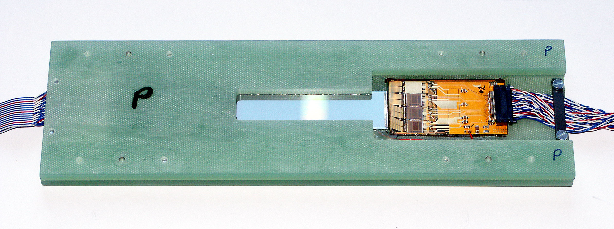
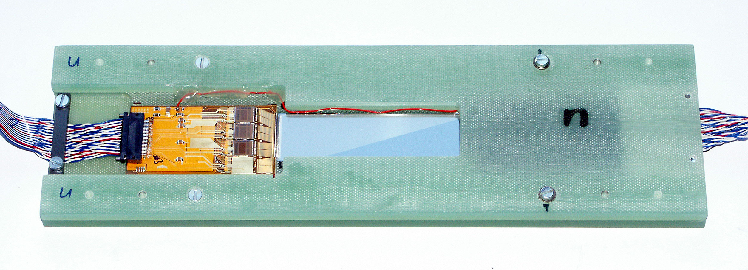
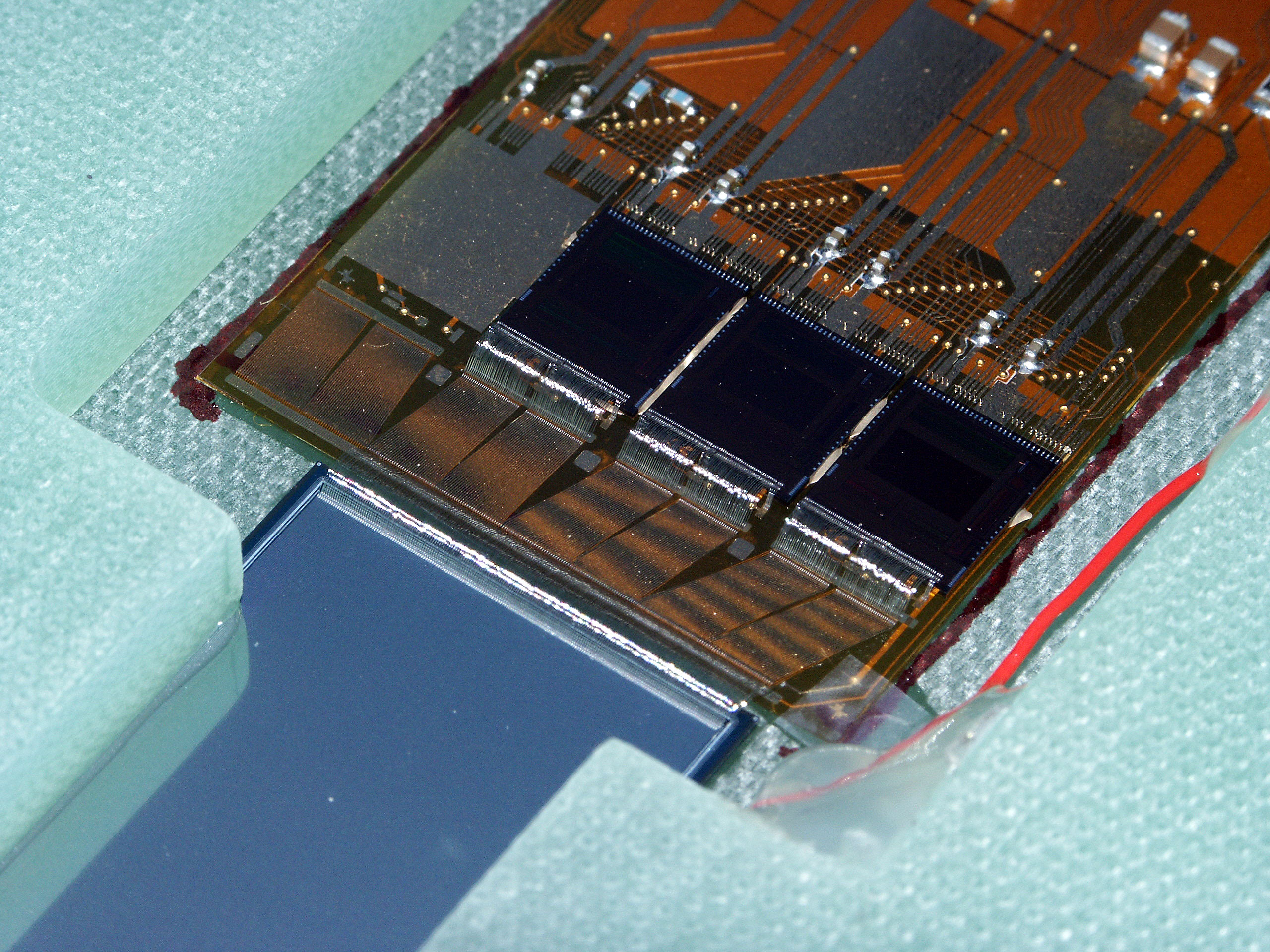
Markus Friedl | BELLE | Micron DDD5 Photos | | | | | This is the new Micron DDD5 double-sided module with 3+3 APV25 readout chips on each side.
The p-side flex hybrid sits at the edge of the sensor, while the n-side flex hybrid is located on top of about
1/3 of the sensor, separated by 1mm of Rohacell.
Sensor data (copied from the Micron catalogue):
DESIGN DDD5 - AC COUPLED ION IMPLANTED TOTALLY DEPLETED DOUBLE SIDED DOUBLE METAL MICROSTRIP DETECTOR
SILICON DETECTOR TYPE: AC coupled ion implanted totally depleted silicon microstrip detector.
DESIGN: Double sided, two metal layers on NN+ 6 inch wafer technology.
JUNCTION SIDE
No STRIPS: 384
STRIP PITCH: 50 �m
OHMIC SIDE
First Metal
No STRIPS: 768
STRIP PITCH: 153.5 �m
Second Metal
No STRIPS: 384
STRIP PITCH: 49.5 �m
POLYSILICON RESISTOR: 2.5 � 0.5 M
COUPLING CAPACITOR: 100 pF
SILICON THICKNESS: 300 � 10 �m
CHIP DIMENSIONS: 120.125 x 21.2 mm2
FULL DEPLETION VOLTAGE (FD): 50 V maximum
OPERATING VOLTAGE: FD to 2FD
EXPERIMENTS: D2, FNAL |
| Attachment 1: micron_pside.jpg
|  |
| Attachment 2: micron_nside.jpg
|  |
| Attachment 3: micron_pside_detail.jpg
|  |
| Attachment 4: micron_nside_detail.jpg
|  |
|
12
|
Fri May 30 10:36:18 2008 |
Marko Dragicevic | other | Important Information/Contact | | | | | IPs
Linksys Router
- external: routerhephy.cern.ch (137.138.171.102)
- internal: 192.168.1.1
US&ER /PA_SS'WD: admin/sensor
- WLAN-SSID: HEPHY
- WLAN-WPA-TKIP: testbeam08
EUDETMAC
- external: eudetmac001.cern.ch
- U1SE*R/P*AS�S/WD (ssh): eudet/gsigsi
- from EUDETMAC to TLU:
ssh tlupc
LAB2PC (APVDAQ, DUT HV)
- internal: 192.168.1.10
- external VNC: routerhephy.cern.ch (137.138.171.102:5900)
pa2s2s2w2d: hephy
XY Table
- internal VNC: 192.168.1.11
pa2s2s2w2d: hephy
Beam Control PC
- external VNC: CWO-HNA453-H6B1.CERN.CH (137.138.61.206)
Phone
Vienna CERN Mobile Phone (usually Thomas Bergauer)
Daniel Haas
Marko Dragicevic
- Hostel (39-120): 79 120
- Private: +43 650 4243343
Markus Friedl
- Hostel (41-107): 60 107
- Private: +43 699 17251085
Thomas Bergauer
- Hostel (39-220): 79 220
- Private: +43 664 3769400 (switched off during testbeam)
Christian Irmler
- Hostel (41-222): 60 222
- Private: +43 699 19437327
Misc
SPS Page 1
Path to start cesar
|
|
34
|
Sun Jun 1 23:36:21 2008 |
Christian Irmler | SiLC | HowTo analyse data | | | | | The analysis consists of two stages:
- The first is zero supression an cluster finding done with "apvdaq_analysis_fadc" (Labwindows/CVI application)
- The second stage is hit time reconstruction done with ROOT. (hitfit)
Both are installed on EUDETMAC.
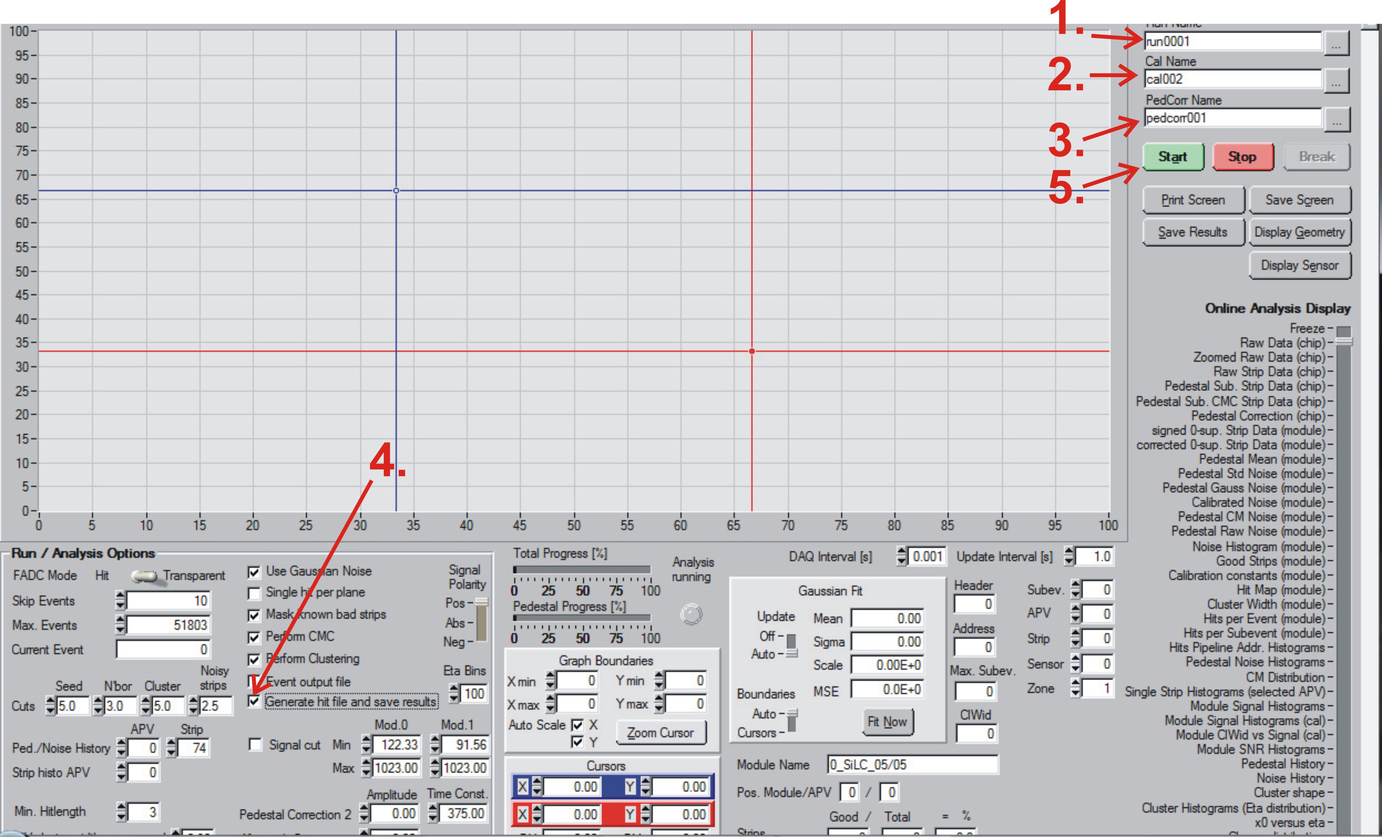
apvdaq_analysis_fadc:
- start apvdaq_analysis_fadc within the virtal Windows XP machine (parallels).
- select a runfile, e.g. run0001.dat
- select a propper calibration file, default is "cal002.out"
- select pedestal correction file, default is "pedcorr001.ped"
- enable "generate hit file and save results"
- click "Start"
- The result of the analyis is a file containing all hits above threshold, the filename is "xxxxxxx_cluster.hit", where xxxxxxx is the run name
- The data structure of the file is described at http://elog.hephy.at/testbeam-SPS08/04
- The file is located in the same folder as the raw data file (= data)
hitfit:
- Once apvdaq_analysis_fadc is finished, start a console window and change into the directory /Volumes/Data/eudet/APVDAQ
- execute ./hitfitrun nnnn, where nnnn is the run number
- results: file with fitted hits (data structure see http://elog.hephy.at/testbeam-SPS08/04) as well as several plots.
- file name: xxxxxxx_cluster.hit.fit, the file is located in the subdirectory output.
|
| Attachment 1: analysis_howto.jpg
|  |
|
11
|
Mon May 26 15:38:53 2008 |
Markus Friedl | SiLC | How to run APVDAQ | | | | | Power-on Procedure
==================
PC logon: user "testbeam", pwd "sensor"
Order for switching on the hardware (not strict):
* VME 9U crate
* keithley instruments
* +-5V (fat) 2 lab power supplies (left stack)
* other 3 lab power supplies (right stack)
BE CAREFUL NOT TO CHANGE DIALS AT ALL DURING SWITCHING!!!
Run ResMan.exe (shortcut on desktop) and click OK to close
Start longterm-R31.vi (shortcut on desktop) and start HV bias
Start APVDAQ.exe
Now everything is on and ready to operate.
This is also the condition after a run is finished.
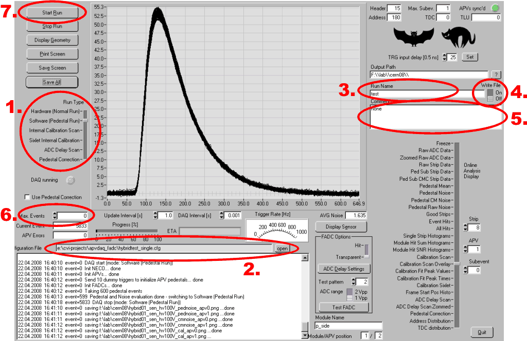
Start Run (see screenshot below)
================================
1. select proper run type (if different from previous run), typically
Hardware (beam) or
Software (pedestal) or
Internal Calibration
2. open proper config file (if different from previous run), one of
cern08_silc_all_single.cfg (8 DUTs, 1 sample) - for software (pedestal) and intcal runs
cern08_silc_all_multi6.cfg (8 DUTs, 6 samples) - for hardware (beam) runs
cern08_silc_mod03_single.cfg (1 DUT, module 03, 1 sample) - for software (pedestal) and intcal runs
cern08_silc_mod03_multi6.cfg (1 DUT, module 03, 6 samples) - for hardware (beam) runs
3. select file name (typically: increase run number)
4. switch Write File ON (if turned off)
5. write some useful comments (conditions, HV, etc)
6. enter number of events
7. hit "Start Run" and relax or cry for help :-)
Additional Info
===============
path to APVDAQ: e:\cvi-projects\apvdaq_fadc
path to Longterm: e:\labview-projects\longterm R3.1
path to data: f:\testbeam\cern_jun08\silc\data |
| Attachment 1: panel_instruction.gif
|  |
| Attachment 2: cern08_silc_all_single.cfg
|
# 40 mhz
# single peak mode (1 sample)
# 50ns peaking time
# 30ns trigger window (built from 5ns window, thus ~12.5ns later)
# NECO
#
# Data processing with FADC+PROC
# SPS Testbeam - full setup
# FADC 0 four hybrids
# FADC 1 four hybrids
#
#
# CI 07 may 2008
#
#
# Lines preceded by a # or ; sign are ignored.
#
# [rem] comments a whole section until the next section start marked by [xxx] .
#
# [vme]
# VME addresses are given in the format
# {module_name} = {vme_module_number},{vme_address_hex}
# nec ... NECO module
# adf ... particular FADC module
#
# Please note that the address ranges are not defined here,
# they are implicitly given by the hardware.
# Module numbers must fill from 0 (this is not checked).
# Please note that no range checking is performed.
# There is no access to VME modules that are not included in this list,
[vme]
nec = 0,0x1a000000
adf = 0,0x1b000000
adf = 1,0x2b000000
# [nec]
# NECO related information
# mod = 0|1,{shift_register_delay},{adc_range},{win_delay},{win_length},{dead_time},{time_lat},{max_trg}
# (default: 0,75,0,50?,900?,36,2,1)
# res = {list of entries in reset sequence} (default: 2,4)
# cal = {list of entries in cal sequence} (default: 2,3,250,251)
# sw5 = {list of entries in single cal sequence} (default: 2,3)
# str = {list of entries in software trigger sequence} (default: 75)
# htr = {list of entries in hardware trigger sequence} (default: 74)
#
# mod specifies to use either the sequencer (0) or the shift register (1) for hardware trigger and the
# delay of the shift register (0..255); adc_range (0=1Vpp, 1=2Vpp) -- ignored; win_delay and win_length define
# the starting point (relative to the APV trigger) and length of the ADC gate in transparent mode; dead_time is
# the number of 254MHz clock cycles which are set to zero for time measurement after an incoming trigger;
# time_lat is the latency for time measurement in terms of 40MHz clock cycles; max_trg is the number of incoming
# triggers which required to activate the veto logic (usually 1; 0 completely disables the veto logic)
# res, cal, sw5, str and htr are containing the bits to set in the 256-element sequencer memory (nothing is set at -1)
# Please note that cal+str together produce a calibration request plus subsequent normal trigger, so the time
# between them is the latency. sw5 is used to send a single cal request to achieve the correct polarity in
# case the APV inverter is turned on (this feature only works for entire MAMBOs halves = groups of 3 REBOs)
#
# These settings are quite fragile! Do not modify until you know exactly what you are doing.
[nec]
# 30m cables, 40mhz, Tp=50ns, single-trigger
#mod = 0,75,0,70,250,36,2,1
#htr = 61,-1,-1,-1,-1,-1,-1,-1
#str = 100,-1,-1,-1,-1,-1,-1,-1
# TESTBEAM Nov 07, 30m cables, 40mhz, Tp=50ns, multi-trigger (6 samples)
#mod = 0,75,0,70,950,36,2,1
#htr = 59,62,-1,-1,-1,-1,-1,-1
#str = 100,103,-1,-1,-1,-1,-1,-1
# SiLC TESTBEAM June 08, 7m sc cables, 30m repeater cables, 40mhz, Tp=50ns, single-trigger (1 samples)
mod = 0,75,0,70,250,36,2,1
htr = 63,-1,-1,-1,-1,-1,-1,-1
str = 100,-1,-1,-1,-1,-1,-1,-1
# SiLC TESTBEAM June 08, 7m sc cables, 30m repeater cables, 40mhz, Tp=50ns, multi-trigger (6 samples)
#mod = 0,75,0,70,950,36,2,1
#htr = 61,64,-1,-1,-1,-1,-1,-1
#str = 100,103,-1,-1,-1,-1,-1,-1
#common settings
res = 2, 4, -1, -1,-1,-1,-1,-1
cal = 2, 3,250,251,-1,-1,-1,-1
sw5 = 2, 3, -1, -1,-1,-1,-1,-1
# [daq]
# DAQ related specifications are given in the format
# ads = {N},{search_max_subevents},0,x
# ini = {initevents},{readout_mode},0,x
# deh = {module_position},{apv_position},0,x
# i2t = {N},0,0,x
# pat = 0,0,0,{data_file_path}
# clk = {N},{Delay25 frequency range},0,x
# pdl = {Trigger input delay},0,0,x
# crd = {crate_number},{clkdel},{trgdel},x
#
# ads N gives the number of samples that are read out from the FIFO1 in transparent mode, search_max_subevents is the
# maximum number of subevents to search for within one ADC stream (default=1).
# ini: initevents is the number of software triggers in the beginning of a run for pedestal and noise
# evaluation. At the beginning of each run, 2*initevents are generated by software, after that the
# selected trigger source (hardware, software of calibration) is activated. The initial evaluation
# events are written to disk as normal events are.
# ini: readout_mode defines whether events beyond the initevents are read in raw transparent mode from FIFO1 (0) or
# in processed mode (1) where only hit information is read from FIFO3
# deh is the APV chip for which single strip histograms are recorded
# i2t is the maximum number of I2C retries in case of failure
# pat specifies the save path for data files (must include a trailing backslash!)
# clk gives the system clock period in integer ns (25 max.) and the frequency range for the Delay25 chip:
# 0...40 MHz, 1...80 MHz, 2...32 MHz, 3...64 MHz
# pdl specifies the delay setting for the trigger input in 0.5ns steps (0..49)
# crd define the global clock and trigger delays between NECO and SVD3_buffer for crates 0 and 1
# NOTE: clock and trigger is NOT propagated to any crate(s) NOT specified here
[daq]
# TESTBEAM Nov 07
#Standard
ads = 250,1,0,x
# TESTBEAM Nov 07
#Multitrigger (6)
#ads = 950,6,0,x
# RAW (transparent mode) readout
ini = 300,0,0,x
# PROCESSED readout
#ini = 300,1,0,x
deh = 1,0,0,x
i2t = 5,0,0,x
pat = 0,0,0,F:\\testbeam\\cern_jun08\\silc\\data\\
#standard 40mhz clock (25ns)
clk = 25,0,0,x
pdl = 25,0,0,x
#crate distribution delays (set to mid-range to allow adjustments in both directions)
crd = 0,25,25,x
#we don't use crate 1, so we don't set any delay here -> no clock/trigger to crate 1
###crd = 1,25,25,x
# [hit]
# Hit recognition variables are specified here
# hcs = {hitcut_seed_strip},{hitcut_neighbor_strips}
# nok = {x.x},0
#
#
# hcs gives seed and neighbor hit cuts in units of strip sigma
# nok states the threshold over average noise at which strips are excluded from further analysis (to exclude noisy strips)
[hit]
# si sensor
hcs = 4.0,4.0
# do not exclude strips
nok = 2000.0,0
# [cal]
# Calibration related data
# lvl = {level},0
# lat = {latbeg},{latend}
# sam = {average_samples},{number of samples in 6-tuple mode}
# grp = {number_of_groups},0
# lg6 = {latency},{group}
# lv6 = {startlevel},{endlevel}
#
# lvl is the CLVL amplitude (0..255), 1 is 625e-, 36 is 1 MIP (22500e-) nominally, in reality 26 is 1 MIP
# lat is the Latency range to cover (latend-latbeg>=2, latend-latbeg<=15)
# sam is the number of samples to average per position for normal and 6-tuple modes
# grp is how many groups to scan (<=8), first group is strips 0,8,16,..., second group is 1,9,17,..., ...
# lg6 defines the latency in 6-tuple mode and which group to observe in that mode
# lv6 defines the scan range of amplitude in 6-tuple mode
[cal]
#real 1 MIP level (22400e)
lvl = 26,0
#real 5 MIPs level
#lvl = 130,0
#LAT=95/98 Calibration (short display)
#lat = 89,100
#LAT=95/98 Calibration (short display for >=50mhz)
#lat = 81,98
#LAT=95/98 Calibration (long peak mode tail display)
lat = 75,100
#common settings
sam = 50,150
grp = 8,0
#6-tuple mode settings
lg6 = 97, 1
#lv6 = 1,95
lv6 = 50,52
# [i2c]
# This section defines one or more I2C sets for the APV25. In the [mod] section, those sets are referenced to by their number.
# ia2 = {number},{mode},{lat},{ipre},{ipcasc},{ipsf},{isha},{issf},{ipsp},{imuxin},{vfp},{vfs},{vpsp},{muxgain}
#
# The I2C settings must be individually numbered (ascending from 0). The easiest case is to use the same
# settings for all chips of one type, but one could go so far to use separate settings for each chip.
# vadj/vpsp is set individually for each apv in the [mod] section, the value specified here is meaningless.
[i2c]
# apv25s1, peak, inverter ON, Tp=50ns, (p side)
ia2 = 0, 63, 95, 98, 52, 34, 34, 34, 55, 34, 30, 60, 0, 4
# apv25s1, peak, inverter OFF, Tp=50ns, (n side)
ia2 = 1, 31, 95, 98, 52, 34, 34, 34, 55, 34, 30, 60, 0, 4
# apv25s1, multi-peak, inverter ON, Tp=50ns, (p side)
#ia2 = 0, 61, 95, 98, 52, 34, 34, 34, 55, 34, 30, 60, 0, 4
# apv25s1, multi-peak, inverter OFF, Tp=50ns, (n side)
#ia2 = 1, 29, 95, 98, 52, 34, 34, 34, 55, 34, 30, 60, 0, 4
# [mod]
# Detector module (actually hybrid) specifications are given in the format
# mod = {module_position},{crate_number},{mambo_number},{rebo_number},{hybrid_number},m,{AD8128_peak},{rebo_clkdelay},{rebo_trgdelay},0,0,0,0,{Name}
# apv = {module_position},{apv_position},{i2c_address},{i2c_settings},{vadj/vpsp},x,0,0,{fadc_offset},{fadc_number},{fadc_channel},{fadc_clkdelay [0..49]},{AD8128_gain},x
#
# mod gives the hybrid/module properties: The position counts from 0 to 7 in beam direction,
# Name must not contain blanks ("_" is allowed).
# apv describes the chips located on a hybrid
# and the ADC channel where they are read out, either a Vienna ADC (a) or a FED (f).
# The ADC offset is only available with the Vienna ADCs and shifts the baseline.
# The individual chip vadj setting dominates over the [i2c] setting.
[mod]
# module 0
mod = 0,0,0,2,0,m,45,25,0,0,0,0,0, 0_SiLC_05/05
apv = 0,0,36,0,30,x,0,0,5,0,1,12,100,x
apv = 0,1,38,0,30,x,0,0,5,0,2,15,100,x
# module 1
mod = 1,0,0,2,1,m,45,25,0,0,0,0,0, 1_SiLC_07/07
apv = 1,0,36,0,30,x,0,0,5,0,5,15,100,x
apv = 1,1,38,0,30,x,0,0,5,0,6,16,100,x
# module 2
mod = 2,0,0,2,2,m,45,25,0,0,0,0,0, 2_SiLC_06/03
apv = 2,0,36,0,30,x,0,0,5,0,9,10,100,x
apv = 2,1,38,0,30,x,0,0,5,0,10,15,100,x
# module 3
mod = 3,0,0,2,3,m,45,25,0,0,0,0,0, 3_SiLC_04/04
apv = 3,0,36,0,30,x,0,0,5,0,13,12,100,x
apv = 3,1,38,0,30,x,0,0,5,0,14,14,100,x
# module 4
mod = 4,0,1,1,0,m,45,25,0,0,0,0,0, 4_SiLC_03/10
apv = 4,0,36,0,30,x,0,0,110,1,1,14,100,x
apv = 4,1,38,0,30,x,0,0,110,1,2,15,100,x
# module 5
mod = 5,0,1,1,1,m,45,25,0,0,0,0,0, 5_SiLC_12/08
apv = 5,0,36,0,30,x,0,0,110,1,5,14,100,x
apv = 5,1,38,0,30,x,0,0,110,1,6,16,100,x
# module 6
mod = 6,0,1,1,2,m,45,25,0,0,0,0,0, 6_SiLC_10/02
apv = 6,0,36,0,30,x,0,0,110,1,9,12,100,x
apv = 6,1,38,0,30,x,0,0,120,1,10,15,100,x
# module 7
mod = 7,0,1,1,3,m,45,25,0,0,0,0,0, 7_SiLC_20/09
apv = 7,0,36,0,30,x,0,0,125,1,13,10,100,x
apv = 7,1,38,0,30,x,0,0,115,1,14,14,100,x
# [bad]
# Bad channels description table
# bad = {module_position},{apv_position},{List of 18 strip values or -1}
#
# Maps bad channels, which are then excluded from hit search. Up to 18 bad strips can be entered per line,
# more lines per APV are allowed. Unused values in the list must be filled with -1
[bad]
#bad = 2,0,73,-1,-1,-1,-1,-1,-1,-1,-1,-1,-1,-1,-1,-1,-1,-1,-1,-1
[sen]
# sensor configuration
# sen = {sensor number},{number strips on p side},{numeration direction p},{number strips on n side},{numeration direction n},{first_full},{last_full},{pitch p [�m]}, {pitch n [�m]},{angle [�]},{height [�m]}
# apv = {sensor number},{module_position},{apv_position},{first_strip},{num_floating},{side},0,0,0,0,0
... 193 more lines ...
|
| Attachment 3: cern08_silc_all_multi6.cfg
|
# 40 mhz
# multi peak mode (6 sample)
# 50ns peaking time
# 30ns trigger window (built from 5ns window, thus ~12.5ns later)
# NECO
#
# Data processing with FADC+PROC
# SPS Testbeam - full setup
# FADC 0 four hybrids
# FADC 1 four hybrids
#
#
# CI 07 may 2008
#
#
# Lines preceded by a # or ; sign are ignored.
#
# [rem] comments a whole section until the next section start marked by [xxx] .
#
# [vme]
# VME addresses are given in the format
# {module_name} = {vme_module_number},{vme_address_hex}
# nec ... NECO module
# adf ... particular FADC module
#
# Please note that the address ranges are not defined here,
# they are implicitly given by the hardware.
# Module numbers must fill from 0 (this is not checked).
# Please note that no range checking is performed.
# There is no access to VME modules that are not included in this list,
[vme]
nec = 0,0x1a000000
adf = 0,0x1b000000
adf = 1,0x2b000000
# [nec]
# NECO related information
# mod = 0|1,{shift_register_delay},{adc_range},{win_delay},{win_length},{dead_time},{time_lat},{max_trg}
# (default: 0,75,0,50?,900?,36,2,1)
# res = {list of entries in reset sequence} (default: 2,4)
# cal = {list of entries in cal sequence} (default: 2,3,250,251)
# sw5 = {list of entries in single cal sequence} (default: 2,3)
# str = {list of entries in software trigger sequence} (default: 75)
# htr = {list of entries in hardware trigger sequence} (default: 74)
#
# mod specifies to use either the sequencer (0) or the shift register (1) for hardware trigger and the
# delay of the shift register (0..255); adc_range (0=1Vpp, 1=2Vpp) -- ignored; win_delay and win_length define
# the starting point (relative to the APV trigger) and length of the ADC gate in transparent mode; dead_time is
# the number of 254MHz clock cycles which are set to zero for time measurement after an incoming trigger;
# time_lat is the latency for time measurement in terms of 40MHz clock cycles; max_trg is the number of incoming
# triggers which required to activate the veto logic (usually 1; 0 completely disables the veto logic)
# res, cal, sw5, str and htr are containing the bits to set in the 256-element sequencer memory (nothing is set at -1)
# Please note that cal+str together produce a calibration request plus subsequent normal trigger, so the time
# between them is the latency. sw5 is used to send a single cal request to achieve the correct polarity in
# case the APV inverter is turned on (this feature only works for entire MAMBOs halves = groups of 3 REBOs)
#
# These settings are quite fragile! Do not modify until you know exactly what you are doing.
[nec]
# 30m cables, 40mhz, Tp=50ns, single-trigger
#mod = 0,75,0,70,250,36,2,1
#htr = 61,-1,-1,-1,-1,-1,-1,-1
#str = 100,-1,-1,-1,-1,-1,-1,-1
# TESTBEAM Nov 07, 30m cables, 40mhz, Tp=50ns, multi-trigger (6 samples)
#mod = 0,75,0,70,950,36,2,1
#htr = 59,62,-1,-1,-1,-1,-1,-1
#str = 100,103,-1,-1,-1,-1,-1,-1
# SiLC TESTBEAM June 08, 7m sc cables, 30m repeater cables, 40mhz, Tp=50ns, multi-trigger (6 samples)
mod = 0,75,0,70,950,36,2,1
htr = 61,64,-1,-1,-1,-1,-1,-1
str = 100,103,-1,-1,-1,-1,-1,-1
#common settings
res = 2, 4, -1, -1,-1,-1,-1,-1
cal = 2, 3,250,251,-1,-1,-1,-1
sw5 = 2, 3, -1, -1,-1,-1,-1,-1
# [daq]
# DAQ related specifications are given in the format
# ads = {N},{search_max_subevents},0,x
# ini = {initevents},{readout_mode},0,x
# deh = {module_position},{apv_position},0,x
# i2t = {N},0,0,x
# pat = 0,0,0,{data_file_path}
# clk = {N},{Delay25 frequency range},0,x
# pdl = {Trigger input delay},0,0,x
# crd = {crate_number},{clkdel},{trgdel},x
#
# ads N gives the number of samples that are read out from the FIFO1 in transparent mode, search_max_subevents is the
# maximum number of subevents to search for within one ADC stream (default=1).
# ini: initevents is the number of software triggers in the beginning of a run for pedestal and noise
# evaluation. At the beginning of each run, 2*initevents are generated by software, after that the
# selected trigger source (hardware, software of calibration) is activated. The initial evaluation
# events are written to disk as normal events are.
# ini: readout_mode defines whether events beyond the initevents are read in raw transparent mode from FIFO1 (0) or
# in processed mode (1) where only hit information is read from FIFO3
# deh is the APV chip for which single strip histograms are recorded
# i2t is the maximum number of I2C retries in case of failure
# pat specifies the save path for data files (must include a trailing backslash!)
# clk gives the system clock period in integer ns (25 max.) and the frequency range for the Delay25 chip:
# 0...40 MHz, 1...80 MHz, 2...32 MHz, 3...64 MHz
# pdl specifies the delay setting for the trigger input in 0.5ns steps (0..49)
# crd define the global clock and trigger delays between NECO and SVD3_buffer for crates 0 and 1
# NOTE: clock and trigger is NOT propagated to any crate(s) NOT specified here
[daq]
# TESTBEAM Nov 07
#Standard
#ads = 250,1,0,x
# TESTBEAM Nov 07
#Multitrigger (6)
ads = 950,6,0,x
# RAW (transparent mode) readout
ini = 300,0,0,x
# PROCESSED readout
#ini = 300,1,0,x
deh = 1,0,0,x
i2t = 5,0,0,x
pat = 0,0,0,F:\\testbeam\\cern_jun08\\silc\\data\\
#standard 40mhz clock (25ns)
clk = 25,0,0,x
pdl = 25,0,0,x
#crate distribution delays (set to mid-range to allow adjustments in both directions)
crd = 0,25,25,x
#we don't use crate 1, so we don't set any delay here -> no clock/trigger to crate 1
###crd = 1,25,25,x
# [hit]
# Hit recognition variables are specified here
# hcs = {hitcut_seed_strip},{hitcut_neighbor_strips}
# nok = {x.x},0
#
#
# hcs gives seed and neighbor hit cuts in units of strip sigma
# nok states the threshold over average noise at which strips are excluded from further analysis (to exclude noisy strips)
[hit]
# si sensor
hcs = 4.0,4.0
# do not exclude strips
nok = 2000.0,0
# [cal]
# Calibration related data
# lvl = {level},0
# lat = {latbeg},{latend}
# sam = {average_samples},{number of samples in 6-tuple mode}
# grp = {number_of_groups},0
# lg6 = {latency},{group}
# lv6 = {startlevel},{endlevel}
#
# lvl is the CLVL amplitude (0..255), 1 is 625e-, 36 is 1 MIP (22500e-) nominally, in reality 26 is 1 MIP
# lat is the Latency range to cover (latend-latbeg>=2, latend-latbeg<=15)
# sam is the number of samples to average per position for normal and 6-tuple modes
# grp is how many groups to scan (<=8), first group is strips 0,8,16,..., second group is 1,9,17,..., ...
# lg6 defines the latency in 6-tuple mode and which group to observe in that mode
# lv6 defines the scan range of amplitude in 6-tuple mode
[cal]
#real 1 MIP level (22400e)
lvl = 26,0
#real 5 MIPs level
#lvl = 130,0
#LAT=95/98 Calibration (short display)
#lat = 89,100
#LAT=95/98 Calibration (short display for >=50mhz)
#lat = 81,98
#LAT=95/98 Calibration (long peak mode tail display)
lat = 75,100
#common settings
sam = 50,150
grp = 8,0
#6-tuple mode settings
lg6 = 97, 1
#lv6 = 1,95
lv6 = 50,52
# [i2c]
# This section defines one or more I2C sets for the APV25. In the [mod] section, those sets are referenced to by their number.
# ia2 = {number},{mode},{lat},{ipre},{ipcasc},{ipsf},{isha},{issf},{ipsp},{imuxin},{vfp},{vfs},{vpsp},{muxgain}
#
# The I2C settings must be individually numbered (ascending from 0). The easiest case is to use the same
# settings for all chips of one type, but one could go so far to use separate settings for each chip.
# vadj/vpsp is set individually for each apv in the [mod] section, the value specified here is meaningless.
[i2c]
# apv25s1, peak, inverter ON, Tp=50ns, (p side)
#ia2 = 0, 63, 95, 98, 52, 34, 34, 34, 55, 34, 30, 60, 0, 4
# apv25s1, peak, inverter OFF, Tp=50ns, (n side)
#ia2 = 1, 31, 95, 98, 52, 34, 34, 34, 55, 34, 30, 60, 0, 4
# apv25s1, multi-peak, inverter ON, Tp=50ns, (p side)
ia2 = 0, 61, 95, 98, 52, 34, 34, 34, 55, 34, 30, 60, 0, 4
# apv25s1, multi-peak, inverter OFF, Tp=50ns, (n side)
ia2 = 1, 29, 95, 98, 52, 34, 34, 34, 55, 34, 30, 60, 0, 4
# [mod]
# Detector module (actually hybrid) specifications are given in the format
# mod = {module_position},{crate_number},{mambo_number},{rebo_number},{hybrid_number},m,{AD8128_peak},{rebo_clkdelay},{rebo_trgdelay},0,0,0,0,{Name}
# apv = {module_position},{apv_position},{i2c_address},{i2c_settings},{vadj/vpsp},x,0,0,{fadc_offset},{fadc_number},{fadc_channel},{fadc_clkdelay [0..49]},{AD8128_gain},x
#
# mod gives the hybrid/module properties: The position counts from 0 to 7 in beam direction,
# Name must not contain blanks ("_" is allowed).
# apv describes the chips located on a hybrid
# and the ADC channel where they are read out, either a Vienna ADC (a) or a FED (f).
# The ADC offset is only available with the Vienna ADCs and shifts the baseline.
# The individual chip vadj setting dominates over the [i2c] setting.
[mod]
# module 0
mod = 0,0,0,2,0,m,45,25,0,0,0,0,0, 0_SiLC_05/05
apv = 0,0,36,0,30,x,0,0,5,0,1,12,100,x
apv = 0,1,38,0,30,x,0,0,5,0,2,15,100,x
# module 1
mod = 1,0,0,2,1,m,45,25,0,0,0,0,0, 1_SiLC_07/07
apv = 1,0,36,0,30,x,0,0,5,0,5,15,100,x
apv = 1,1,38,0,30,x,0,0,5,0,6,16,100,x
# module 2
mod = 2,0,0,2,2,m,45,25,0,0,0,0,0, 2_SiLC_06/03
apv = 2,0,36,0,30,x,0,0,5,0,9,10,100,x
apv = 2,1,38,0,30,x,0,0,5,0,10,15,100,x
# module 3
mod = 3,0,0,2,3,m,45,25,0,0,0,0,0, 3_SiLC_04/04
apv = 3,0,36,0,30,x,0,0,5,0,13,12,100,x
apv = 3,1,38,0,30,x,0,0,5,0,14,14,100,x
# module 4
mod = 4,0,1,1,0,m,45,25,0,0,0,0,0, 4_SiLC_03/10
apv = 4,0,36,0,30,x,0,0,110,1,1,14,100,x
apv = 4,1,38,0,30,x,0,0,110,1,2,15,100,x
# module 5
mod = 5,0,1,1,1,m,45,25,0,0,0,0,0, 5_SiLC_12/08
apv = 5,0,36,0,30,x,0,0,110,1,5,14,100,x
apv = 5,1,38,0,30,x,0,0,110,1,6,16,100,x
# module 6
mod = 6,0,1,1,2,m,45,25,0,0,0,0,0, 6_SiLC_10/02
apv = 6,0,36,0,30,x,0,0,110,1,9,12,100,x
apv = 6,1,38,0,30,x,0,0,120,1,10,15,100,x
# module 7
mod = 7,0,1,1,3,m,45,25,0,0,0,0,0, 7_SiLC_20/09
apv = 7,0,36,0,30,x,0,0,125,1,13,10,100,x
apv = 7,1,38,0,30,x,0,0,115,1,14,14,100,x
# [bad]
# Bad channels description table
# bad = {module_position},{apv_position},{List of 18 strip values or -1}
#
# Maps bad channels, which are then excluded from hit search. Up to 18 bad strips can be entered per line,
# more lines per APV are allowed. Unused values in the list must be filled with -1
[bad]
#bad = 2,0,73,-1,-1,-1,-1,-1,-1,-1,-1,-1,-1,-1,-1,-1,-1,-1,-1,-1
[sen]
# sensor configuration
# sen = {sensor number},{number strips on p side},{numeration direction p},{number strips on n side},{numeration direction n},{first_full},{last_full},{pitch p [�m]}, {pitch n [�m]},{angle [�]},{height [�m]}
# apv = {sensor number},{module_position},{apv_position},{first_strip},{num_floating},{side},0,0,0,0,0
# zon = {sensor number},{zone number},{first strip on p side},{last strip on p side},{first strip on n side},{last strip on n side},0,0,0,0,0
#
# sen defines the sensor proberties:
# numeration direction can be 0 = from left to right or 1 = from right to left
#
# apv describes the apvs connected to the sensor
... 187 more lines ...
|
| Attachment 4: cern08_silc_mod03_single.cfg
|
# 40 mhz
# single peak mode (1 sample)
# 50ns peaking time
# 30ns trigger window (built from 5ns window, thus ~12.5ns later)
# NECO
#
# Data processing with FADC+PROC
# SPS Testbeam - single module
# FADC 0 one module at position 3
# FADC 1 not used
#
#
# CI 07 may 2008
#
#
# Lines preceded by a # or ; sign are ignored.
#
# [rem] comments a whole section until the next section start marked by [xxx] .
#
# [vme]
# VME addresses are given in the format
# {module_name} = {vme_module_number},{vme_address_hex}
# nec ... NECO module
# adf ... particular FADC module
#
# Please note that the address ranges are not defined here,
# they are implicitly given by the hardware.
# Module numbers must fill from 0 (this is not checked).
# Please note that no range checking is performed.
# There is no access to VME modules that are not included in this list,
[vme]
nec = 0,0x1a000000
adf = 0,0x1b000000
#adf = 1,0x2b000000
# [nec]
# NECO related information
# mod = 0|1,{shift_register_delay},{adc_range},{win_delay},{win_length},{dead_time},{time_lat},{max_trg}
# (default: 0,75,0,50?,900?,36,2,1)
# res = {list of entries in reset sequence} (default: 2,4)
# cal = {list of entries in cal sequence} (default: 2,3,250,251)
# sw5 = {list of entries in single cal sequence} (default: 2,3)
# str = {list of entries in software trigger sequence} (default: 75)
# htr = {list of entries in hardware trigger sequence} (default: 74)
#
# mod specifies to use either the sequencer (0) or the shift register (1) for hardware trigger and the
# delay of the shift register (0..255); adc_range (0=1Vpp, 1=2Vpp) -- ignored; win_delay and win_length define
# the starting point (relative to the APV trigger) and length of the ADC gate in transparent mode; dead_time is
# the number of 254MHz clock cycles which are set to zero for time measurement after an incoming trigger;
# time_lat is the latency for time measurement in terms of 40MHz clock cycles; max_trg is the number of incoming
# triggers which required to activate the veto logic (usually 1; 0 completely disables the veto logic)
# res, cal, sw5, str and htr are containing the bits to set in the 256-element sequencer memory (nothing is set at -1)
# Please note that cal+str together produce a calibration request plus subsequent normal trigger, so the time
# between them is the latency. sw5 is used to send a single cal request to achieve the correct polarity in
# case the APV inverter is turned on (this feature only works for entire MAMBOs halves = groups of 3 REBOs)
#
# These settings are quite fragile! Do not modify until you know exactly what you are doing.
[nec]
# 30m cables, 40mhz, Tp=50ns, single-trigger
#mod = 0,75,0,70,250,36,2,1
#htr = 61,-1,-1,-1,-1,-1,-1,-1
#str = 100,-1,-1,-1,-1,-1,-1,-1
# TESTBEAM Nov 07, 30m cables, 40mhz, Tp=50ns, multi-trigger (6 samples)
#mod = 0,75,0,70,950,36,2,1
#htr = 59,62,-1,-1,-1,-1,-1,-1
#str = 100,103,-1,-1,-1,-1,-1,-1
# SiLC TESTBEAM June 08, 7m sc cables, 30m repeater cables, 40mhz, Tp=50ns, single-trigger (1 samples)
mod = 0,75,0,70,250,36,2,1
htr = 63,-1,-1,-1,-1,-1,-1,-1
str = 100,-1,-1,-1,-1,-1,-1,-1
# SiLC TESTBEAM June 08, 7m sc cables, 30m repeater cables, 40mhz, Tp=50ns, multi-trigger (6 samples)
#mod = 0,75,0,70,950,36,2,1
#htr = 61,64,-1,-1,-1,-1,-1,-1
#str = 100,103,-1,-1,-1,-1,-1,-1
#common settings
res = 2, 4, -1, -1,-1,-1,-1,-1
cal = 2, 3,250,251,-1,-1,-1,-1
sw5 = 2, 3, -1, -1,-1,-1,-1,-1
# [daq]
# DAQ related specifications are given in the format
# ads = {N},{search_max_subevents},0,x
# ini = {initevents},{readout_mode},0,x
# deh = {module_position},{apv_position},0,x
# i2t = {N},0,0,x
# pat = 0,0,0,{data_file_path}
# clk = {N},{Delay25 frequency range},0,x
# pdl = {Trigger input delay},0,0,x
# crd = {crate_number},{clkdel},{trgdel},x
#
# ads N gives the number of samples that are read out from the FIFO1 in transparent mode, search_max_subevents is the
# maximum number of subevents to search for within one ADC stream (default=1).
# ini: initevents is the number of software triggers in the beginning of a run for pedestal and noise
# evaluation. At the beginning of each run, 2*initevents are generated by software, after that the
# selected trigger source (hardware, software of calibration) is activated. The initial evaluation
# events are written to disk as normal events are.
# ini: readout_mode defines whether events beyond the initevents are read in raw transparent mode from FIFO1 (0) or
# in processed mode (1) where only hit information is read from FIFO3
# deh is the APV chip for which single strip histograms are recorded
# i2t is the maximum number of I2C retries in case of failure
# pat specifies the save path for data files (must include a trailing backslash!)
# clk gives the system clock period in integer ns (25 max.) and the frequency range for the Delay25 chip:
# 0...40 MHz, 1...80 MHz, 2...32 MHz, 3...64 MHz
# pdl specifies the delay setting for the trigger input in 0.5ns steps (0..49)
# crd define the global clock and trigger delays between NECO and SVD3_buffer for crates 0 and 1
# NOTE: clock and trigger is NOT propagated to any crate(s) NOT specified here
[daq]
# TESTBEAM Nov 07
#Standard
ads = 250,1,0,x
# TESTBEAM Nov 07
#Multitrigger (6)
#ads = 950,6,0,x
# RAW (transparent mode) readout
ini = 300,0,0,x
# PROCESSED readout
#ini = 300,1,0,x
deh = 1,0,0,x
i2t = 5,0,0,x
pat = 0,0,0,F:\\testbeam\\cern_jun08\\silc\\data\\
#standard 40mhz clock (25ns)
clk = 25,0,0,x
pdl = 25,0,0,x
#crate distribution delays (set to mid-range to allow adjustments in both directions)
crd = 0,25,25,x
#we don't use crate 1, so we don't set any delay here -> no clock/trigger to crate 1
###crd = 1,25,25,x
# [hit]
# Hit recognition variables are specified here
# hcs = {hitcut_seed_strip},{hitcut_neighbor_strips}
# nok = {x.x},0
#
#
# hcs gives seed and neighbor hit cuts in units of strip sigma
# nok states the threshold over average noise at which strips are excluded from further analysis (to exclude noisy strips)
[hit]
# si sensor
hcs = 4.0,4.0
# do not exclude strips
nok = 2000.0,0
# [cal]
# Calibration related data
# lvl = {level},0
# lat = {latbeg},{latend}
# sam = {average_samples},{number of samples in 6-tuple mode}
# grp = {number_of_groups},0
# lg6 = {latency},{group}
# lv6 = {startlevel},{endlevel}
#
# lvl is the CLVL amplitude (0..255), 1 is 625e-, 36 is 1 MIP (22500e-) nominally, in reality 26 is 1 MIP
# lat is the Latency range to cover (latend-latbeg>=2, latend-latbeg<=15)
# sam is the number of samples to average per position for normal and 6-tuple modes
# grp is how many groups to scan (<=8), first group is strips 0,8,16,..., second group is 1,9,17,..., ...
# lg6 defines the latency in 6-tuple mode and which group to observe in that mode
# lv6 defines the scan range of amplitude in 6-tuple mode
[cal]
#real 1 MIP level (22400e)
lvl = 26,0
#real 5 MIPs level
#lvl = 130,0
#LAT=95/98 Calibration (short display)
#lat = 89,100
#LAT=95/98 Calibration (short display for >=50mhz)
#lat = 81,98
#LAT=95/98 Calibration (long peak mode tail display)
lat = 75,100
#common settings
sam = 50,150
grp = 8,0
#6-tuple mode settings
lg6 = 97, 1
#lv6 = 1,95
lv6 = 50,52
# [i2c]
# This section defines one or more I2C sets for the APV25. In the [mod] section, those sets are referenced to by their number.
# ia2 = {number},{mode},{lat},{ipre},{ipcasc},{ipsf},{isha},{issf},{ipsp},{imuxin},{vfp},{vfs},{vpsp},{muxgain}
#
# The I2C settings must be individually numbered (ascending from 0). The easiest case is to use the same
# settings for all chips of one type, but one could go so far to use separate settings for each chip.
# vadj/vpsp is set individually for each apv in the [mod] section, the value specified here is meaningless.
[i2c]
# apv25s1, peak, inverter ON, Tp=50ns, (p side)
ia2 = 0, 63, 95, 98, 52, 34, 34, 34, 55, 34, 30, 60, 0, 4
# apv25s1, peak, inverter OFF, Tp=50ns, (n side)
ia2 = 1, 31, 95, 98, 52, 34, 34, 34, 55, 34, 30, 60, 0, 4
# apv25s1, multi-peak, inverter ON, Tp=50ns, (p side)
#ia2 = 0, 61, 95, 98, 52, 34, 34, 34, 55, 34, 30, 60, 0, 4
# apv25s1, multi-peak, inverter OFF, Tp=50ns, (n side)
#ia2 = 1, 29, 95, 98, 52, 34, 34, 34, 55, 34, 30, 60, 0, 4
# [mod]
# Detector module (actually hybrid) specifications are given in the format
# mod = {module_position},{crate_number},{mambo_number},{rebo_number},{hybrid_number},m,{AD8128_peak},{rebo_clkdelay},{rebo_trgdelay},0,0,0,0,{Name}
# apv = {module_position},{apv_position},{i2c_address},{i2c_settings},{vadj/vpsp},x,0,0,{fadc_offset},{fadc_number},{fadc_channel},{fadc_clkdelay [0..49]},{AD8128_gain},x
#
# mod gives the hybrid/module properties: The position counts from 0 to 7 in beam direction,
# Name must not contain blanks ("_" is allowed).
# apv describes the chips located on a hybrid
# and the ADC channel where they are read out, either a Vienna ADC (a) or a FED (f).
# The ADC offset is only available with the Vienna ADCs and shifts the baseline.
# The individual chip vadj setting dominates over the [i2c] setting.
[mod]
# module 3
mod = 3,0,0,2,3,m,45,25,0,0,0,0,0, 3_SiLC_04/04
apv = 3,0,36,0,30,x,0,0,5,0,13,12,100,x
apv = 3,1,38,0,30,x,0,0,5,0,14,14,100,x
# [bad]
# Bad channels description table
# bad = {module_position},{apv_position},{List of 18 strip values or -1}
#
# Maps bad channels, which are then excluded from hit search. Up to 18 bad strips can be entered per line,
# more lines per APV are allowed. Unused values in the list must be filled with -1
[bad]
#bad = 2,0,73,-1,-1,-1,-1,-1,-1,-1,-1,-1,-1,-1,-1,-1,-1,-1,-1,-1
[sen]
# sensor configuration
# sen = {sensor number},{number strips on p side},{numeration direction p},{number strips on n side},{numeration direction n},{first_full},{last_full},{pitch p [�m]}, {pitch n [�m]},{angle [�]},{height [�m]}
# apv = {sensor number},{module_position},{apv_position},{first_strip},{num_floating},{side},0,0,0,0,0
# zon = {sensor number},{zone number},{first strip on p side},{last strip on p side},{first strip on n side},{last strip on n side},0,0,0,0,0
#
# sen defines the sensor proberties:
# numeration direction can be 0 = from left to right or 1 = from right to left
#
# apv describes the apvs connected to the sensor
# module_position and apv_position must be identical to the values in section [mod]
# first_strip is the strip number bonded to channel 0
# num_floating is the number of floating strips between two apv channels, set it to 0 if all strips are bonded.
# side: 0 = the apv is bonded to the n side of the sensor
# 1 = the apv is bonded to the p side of the sensor
#
# zon defines zones of strips with similar properties, e.g.bonding density
# for each zone the data should be processed separately
# zone number: this is the number of the zone on one sensor
# module 3
sen = 1,256,0,256,0,0,256,50.0,50.0,90,12750.0
apv = 1,3,0,0,0,1,0,0,0,0,0
apv = 1,3,1,128,0,1,0,0,0,0,0
zon = 1,1,0,15,0,0,0,0,0,0,0
zon = 1,2,16,31,0,0,0,0,0,0,0
zon = 1,3,32,47,0,0,0,0,0,0,0
zon = 1,4,48,63,0,0,0,0,0,0,0
zon = 1,5,64,79,0,0,0,0,0,0,0
zon = 1,6,80,95,0,0,0,0,0,0,0
... 11 more lines ...
|
| Attachment 5: cern08_silc_mod03_multi6.cfg
|
# 40 mhz
# multi peak mode (6 sample)
# 50ns peaking time
# 30ns trigger window (built from 5ns window, thus ~12.5ns later)
# NECO
#
# Data processing with FADC+PROC
# SPS Testbeam - single module
# FADC 0 one module at position 3
# FADC 1 not used
#
#
# CI 07 may 2008
#
#
# Lines preceded by a # or ; sign are ignored.
#
# [rem] comments a whole section until the next section start marked by [xxx] .
#
# [vme]
# VME addresses are given in the format
# {module_name} = {vme_module_number},{vme_address_hex}
# nec ... NECO module
# adf ... particular FADC module
#
# Please note that the address ranges are not defined here,
# they are implicitly given by the hardware.
# Module numbers must fill from 0 (this is not checked).
# Please note that no range checking is performed.
# There is no access to VME modules that are not included in this list,
[vme]
nec = 0,0x1a000000
adf = 0,0x1b000000
#adf = 1,0x2b000000
# [nec]
# NECO related information
# mod = 0|1,{shift_register_delay},{adc_range},{win_delay},{win_length},{dead_time},{time_lat},{max_trg}
# (default: 0,75,0,50?,900?,36,2,1)
# res = {list of entries in reset sequence} (default: 2,4)
# cal = {list of entries in cal sequence} (default: 2,3,250,251)
# sw5 = {list of entries in single cal sequence} (default: 2,3)
# str = {list of entries in software trigger sequence} (default: 75)
# htr = {list of entries in hardware trigger sequence} (default: 74)
#
# mod specifies to use either the sequencer (0) or the shift register (1) for hardware trigger and the
# delay of the shift register (0..255); adc_range (0=1Vpp, 1=2Vpp) -- ignored; win_delay and win_length define
# the starting point (relative to the APV trigger) and length of the ADC gate in transparent mode; dead_time is
# the number of 254MHz clock cycles which are set to zero for time measurement after an incoming trigger;
# time_lat is the latency for time measurement in terms of 40MHz clock cycles; max_trg is the number of incoming
# triggers which required to activate the veto logic (usually 1; 0 completely disables the veto logic)
# res, cal, sw5, str and htr are containing the bits to set in the 256-element sequencer memory (nothing is set at -1)
# Please note that cal+str together produce a calibration request plus subsequent normal trigger, so the time
# between them is the latency. sw5 is used to send a single cal request to achieve the correct polarity in
# case the APV inverter is turned on (this feature only works for entire MAMBOs halves = groups of 3 REBOs)
#
# These settings are quite fragile! Do not modify until you know exactly what you are doing.
[nec]
# 30m cables, 40mhz, Tp=50ns, single-trigger
#mod = 0,75,0,70,250,36,2,1
#htr = 61,-1,-1,-1,-1,-1,-1,-1
#str = 100,-1,-1,-1,-1,-1,-1,-1
# TESTBEAM Nov 07, 30m cables, 40mhz, Tp=50ns, multi-trigger (6 samples)
#mod = 0,75,0,70,950,36,2,1
#htr = 59,62,-1,-1,-1,-1,-1,-1
#str = 100,103,-1,-1,-1,-1,-1,-1
# SiLC TESTBEAM June 08, 7m sc cables, 30m repeater cables, 40mhz, Tp=50ns, multi-trigger (6 samples)
mod = 0,75,0,70,950,36,2,1
htr = 61,64,-1,-1,-1,-1,-1,-1
str = 100,103,-1,-1,-1,-1,-1,-1
#common settings
res = 2, 4, -1, -1,-1,-1,-1,-1
cal = 2, 3,250,251,-1,-1,-1,-1
sw5 = 2, 3, -1, -1,-1,-1,-1,-1
# [daq]
# DAQ related specifications are given in the format
# ads = {N},{search_max_subevents},0,x
# ini = {initevents},{readout_mode},0,x
# deh = {module_position},{apv_position},0,x
# i2t = {N},0,0,x
# pat = 0,0,0,{data_file_path}
# clk = {N},{Delay25 frequency range},0,x
# pdl = {Trigger input delay},0,0,x
# crd = {crate_number},{clkdel},{trgdel},x
#
# ads N gives the number of samples that are read out from the FIFO1 in transparent mode, search_max_subevents is the
# maximum number of subevents to search for within one ADC stream (default=1).
# ini: initevents is the number of software triggers in the beginning of a run for pedestal and noise
# evaluation. At the beginning of each run, 2*initevents are generated by software, after that the
# selected trigger source (hardware, software of calibration) is activated. The initial evaluation
# events are written to disk as normal events are.
# ini: readout_mode defines whether events beyond the initevents are read in raw transparent mode from FIFO1 (0) or
# in processed mode (1) where only hit information is read from FIFO3
# deh is the APV chip for which single strip histograms are recorded
# i2t is the maximum number of I2C retries in case of failure
# pat specifies the save path for data files (must include a trailing backslash!)
# clk gives the system clock period in integer ns (25 max.) and the frequency range for the Delay25 chip:
# 0...40 MHz, 1...80 MHz, 2...32 MHz, 3...64 MHz
# pdl specifies the delay setting for the trigger input in 0.5ns steps (0..49)
# crd define the global clock and trigger delays between NECO and SVD3_buffer for crates 0 and 1
# NOTE: clock and trigger is NOT propagated to any crate(s) NOT specified here
[daq]
# TESTBEAM Nov 07
#Standard
#ads = 250,1,0,x
# TESTBEAM Nov 07
#Multitrigger (6)
ads = 950,6,0,x
# RAW (transparent mode) readout
ini = 300,0,0,x
# PROCESSED readout
#ini = 300,1,0,x
deh = 1,0,0,x
i2t = 5,0,0,x
pat = 0,0,0,F:\\testbeam\\cern_jun08\\silc\\data\\
#standard 40mhz clock (25ns)
clk = 25,0,0,x
pdl = 25,0,0,x
#crate distribution delays (set to mid-range to allow adjustments in both directions)
crd = 0,25,25,x
#we don't use crate 1, so we don't set any delay here -> no clock/trigger to crate 1
###crd = 1,25,25,x
# [hit]
# Hit recognition variables are specified here
# hcs = {hitcut_seed_strip},{hitcut_neighbor_strips}
# nok = {x.x},0
#
#
# hcs gives seed and neighbor hit cuts in units of strip sigma
# nok states the threshold over average noise at which strips are excluded from further analysis (to exclude noisy strips)
[hit]
# si sensor
hcs = 4.0,4.0
# do not exclude strips
nok = 2000.0,0
# [cal]
# Calibration related data
# lvl = {level},0
# lat = {latbeg},{latend}
# sam = {average_samples},{number of samples in 6-tuple mode}
# grp = {number_of_groups},0
# lg6 = {latency},{group}
# lv6 = {startlevel},{endlevel}
#
# lvl is the CLVL amplitude (0..255), 1 is 625e-, 36 is 1 MIP (22500e-) nominally, in reality 26 is 1 MIP
# lat is the Latency range to cover (latend-latbeg>=2, latend-latbeg<=15)
# sam is the number of samples to average per position for normal and 6-tuple modes
# grp is how many groups to scan (<=8), first group is strips 0,8,16,..., second group is 1,9,17,..., ...
# lg6 defines the latency in 6-tuple mode and which group to observe in that mode
# lv6 defines the scan range of amplitude in 6-tuple mode
[cal]
#real 1 MIP level (22400e)
lvl = 26,0
#real 5 MIPs level
#lvl = 130,0
#LAT=95/98 Calibration (short display)
#lat = 89,100
#LAT=95/98 Calibration (short display for >=50mhz)
#lat = 81,98
#LAT=95/98 Calibration (long peak mode tail display)
lat = 75,100
#common settings
sam = 50,150
grp = 8,0
#6-tuple mode settings
lg6 = 97, 1
#lv6 = 1,95
lv6 = 50,52
# [i2c]
# This section defines one or more I2C sets for the APV25. In the [mod] section, those sets are referenced to by their number.
# ia2 = {number},{mode},{lat},{ipre},{ipcasc},{ipsf},{isha},{issf},{ipsp},{imuxin},{vfp},{vfs},{vpsp},{muxgain}
#
# The I2C settings must be individually numbered (ascending from 0). The easiest case is to use the same
# settings for all chips of one type, but one could go so far to use separate settings for each chip.
# vadj/vpsp is set individually for each apv in the [mod] section, the value specified here is meaningless.
[i2c]
# apv25s1, peak, inverter ON, Tp=50ns, (p side)
#ia2 = 0, 63, 95, 98, 52, 34, 34, 34, 55, 34, 30, 60, 0, 4
# apv25s1, peak, inverter OFF, Tp=50ns, (n side)
#ia2 = 1, 31, 95, 98, 52, 34, 34, 34, 55, 34, 30, 60, 0, 4
# apv25s1, multi-peak, inverter ON, Tp=50ns, (p side)
ia2 = 0, 61, 95, 98, 52, 34, 34, 34, 55, 34, 30, 60, 0, 4
# apv25s1, multi-peak, inverter OFF, Tp=50ns, (n side)
ia2 = 1, 29, 95, 98, 52, 34, 34, 34, 55, 34, 30, 60, 0, 4
# [mod]
# Detector module (actually hybrid) specifications are given in the format
# mod = {module_position},{crate_number},{mambo_number},{rebo_number},{hybrid_number},m,{AD8128_peak},{rebo_clkdelay},{rebo_trgdelay},0,0,0,0,{Name}
# apv = {module_position},{apv_position},{i2c_address},{i2c_settings},{vadj/vpsp},x,0,0,{fadc_offset},{fadc_number},{fadc_channel},{fadc_clkdelay [0..49]},{AD8128_gain},x
#
# mod gives the hybrid/module properties: The position counts from 0 to 7 in beam direction,
# Name must not contain blanks ("_" is allowed).
# apv describes the chips located on a hybrid
# and the ADC channel where they are read out, either a Vienna ADC (a) or a FED (f).
# The ADC offset is only available with the Vienna ADCs and shifts the baseline.
# The individual chip vadj setting dominates over the [i2c] setting.
[mod]
# module 3
mod = 3,0,0,2,3,m,45,25,0,0,0,0,0, 3_SiLC_04/04
apv = 3,0,36,0,30,x,0,0,5,0,13,12,100,x
apv = 3,1,38,0,30,x,0,0,5,0,14,14,100,x
# [bad]
# Bad channels description table
# bad = {module_position},{apv_position},{List of 18 strip values or -1}
#
# Maps bad channels, which are then excluded from hit search. Up to 18 bad strips can be entered per line,
# more lines per APV are allowed. Unused values in the list must be filled with -1
[bad]
#bad = 2,0,73,-1,-1,-1,-1,-1,-1,-1,-1,-1,-1,-1,-1,-1,-1,-1,-1,-1
[sen]
# sensor configuration
# sen = {sensor number},{number strips on p side},{numeration direction p},{number strips on n side},{numeration direction n},{first_full},{last_full},{pitch p [�m]}, {pitch n [�m]},{angle [�]},{height [�m]}
# apv = {sensor number},{module_position},{apv_position},{first_strip},{num_floating},{side},0,0,0,0,0
# zon = {sensor number},{zone number},{first strip on p side},{last strip on p side},{first strip on n side},{last strip on n side},0,0,0,0,0
#
# sen defines the sensor proberties:
# numeration direction can be 0 = from left to right or 1 = from right to left
#
# apv describes the apvs connected to the sensor
# module_position and apv_position must be identical to the values in section [mod]
# first_strip is the strip number bonded to channel 0
# num_floating is the number of floating strips between two apv channels, set it to 0 if all strips are bonded.
# side: 0 = the apv is bonded to the n side of the sensor
# 1 = the apv is bonded to the p side of the sensor
#
# zon defines zones of strips with similar properties, e.g.bonding density
# for each zone the data should be processed separately
# zone number: this is the number of the zone on one sensor
# module 3
sen = 1,256,0,256,0,0,256,50.0,50.0,90,12750.0
apv = 1,3,0,0,0,1,0,0,0,0,0
apv = 1,3,1,128,0,1,0,0,0,0,0
zon = 1,1,0,15,0,0,0,0,0,0,0
zon = 1,2,16,31,0,0,0,0,0,0,0
zon = 1,3,32,47,0,0,0,0,0,0,0
zon = 1,4,48,63,0,0,0,0,0,0,0
zon = 1,5,64,79,0,0,0,0,0,0,0
zon = 1,6,80,95,0,0,0,0,0,0,0
zon = 1,7,96,111,0,0,0,0,0,0,0
zon = 1,8,112,127,0,0,0,0,0,0,0
zon = 1,9,128,143,0,0,0,0,0,0,0
zon = 1,10,144,159,0,0,0,0,0,0,0
zon = 1,11,160,175,0,0,0,0,0,0,0
zon = 1,12,176,191,0,0,0,0,0,0,0
zon = 1,13,192,207,0,0,0,0,0,0,0
... 5 more lines ...
|
|
1
|
Tue May 6 13:51:43 2008 |
Thomas Bergauer | other | Equipment list | | | | | Slow Control:
K2410 SMU
K2700 Scanning Voltmeter
Shut-Widerstand-Platine
Flachbandkabel
TRHX + 2 Sensoren + Kabel
Koax-Kabel + Adapter auf Banane
LV-Power-Supplies
Die Katze (Belle-HV-Supply)
DAQ:
Chrisu-PC (inkl. Keyboard, Maus, 2 Monitore)
9U-VME-Crate samt Modulen und PS
DOCK-Box
VME-Kabel (bockig)
30m-Kabel (8xCat7, 2xCat5, 2xgrau)
Lemo-Kabel
100pin-Flachkabel
Bananenkabel
Hybridkabel
Special TLU-Adapter (flipping pin order of RJ45)
Schrauben f�r Crate-Montage
DUT:
9 SiLC-Module
Micron-Modul
3 Belle-Module + Rahmen
Schrauben f�r Montage am Drehteller
EDV:
Netzwerkkabel
Netzwerk-Switch
WLAN-Router WRT54GL
1TB externe Festplatte
Webcam
USB-Stick
Tools:
Scope + 4 Probes
Diverse Adaptoren Lemo-BNC, Lemo-Lemo
Taschenlampe
Massband
Multimeter
Werkzeug (Schraubenzieher & Co)
Pinzetten
Laserpointer
Schwarze Fetzen
Scotch tape
Kabelbinder
Adapter f. Steckdosen falls erforderlich
Verteiler-Leisten
Tixo klein & gross
Misc:
5 pcs. SiLC Alignment Sensors for Marcos Fernandez Garcia
Fondueset 
Digitalkamera
Akkus+Ladeger�t
Dickes Logbook
Kugelschreiber/Bleistifte
Pflaster
VME-6U-PS zur Reparatur
2 x Pixel-FED f�r W.J. & D.K. |
|
2
|
Wed May 7 10:43:09 2008 |
Thomas Bergauer | SiLC | Documentation: twiki, Stephans Hardware Drawings,.... | | | | | DUT, APVDAQ Documentation
CERN TWiki: https://twiki.cern.ch/twiki/bin/view/Main/SiLCTestbeam
Stephan's Documentation: http://wwwhephy.oeaw.ac.at/u3w/s/shaensel/www/HEPHY-Testbeam08/
Telescope:
EUDAQ @ hepforge
LCIO homepage at DESY
JRA1 Meeting with Software tutorial (siehe "Software Session" -> "EUtelescope Tutorial") |
|
4
|
Fri May 9 11:46:36 2008 |
Markus Friedl | SiLC | Data file format | (work in progress) | | | | APVDAQ Data Analysis
====================
The Vienna APVDAQ system has its origin in the late 1990s, and has grown and been improved since then.
Along with the hardware, also the software has grown and hence now consists of several steps rather
than a single piece of software.
DAQ and Analysis Chain
----------------------
Step 0: APVDAQ Software (=online) - CVI/LabWindows under Windows
* controls and reads hardware, provides quick online analysis for online data quality check
* can record software (pedestal), hardware (normal) or calibration runs
* saves raw data (default) or hardware-zero-suppressed data
Step 1: APVDAQ_Analysis - CVI/Labwindows under Windows
* essentially an improved version of step 0, reads step 0 data from file and performs pedestal
subtraction, common-mode correction, hit finding and clump finding (=2D-clustering; we record
typically 6 samples along the shaped waveform for each event for later peak time reconstruction;
thus clustering is not only done along strip axis, but also in time -> we search for contiguous
hit clouds within the two-dimensional x-t-domain and sum up the cluster for each time point)
* saves clustered waveform hit data (typically 6 sampled values per hit)
Step 2: hitfitgui - ROOT under Linux
* reads the clustered waveform hit data from step 1 and performs a waveform fit for each hit with the
reference waveform created from calibration data, resulting in peak amplitude and peak time for each
hit which is compared to a reference time obtained with a TDC (included in the APVDAQ hardware)
* saves peak amplitude and time information per hit
Step 3: anarun.C - ROOT under Linux
* reads the hit properties file from the previous step and fills the data into several histograms like
Signal, SNR, Noise, Cluster Width, Eta distribution etc. for subsequent graphical display, including
Landau*Gauss fits and p-n side correlations
* saves several plot canvasses as PS files
What we don't have
------------------
Tracking, alignment and such things. I think that the best starting point for these functions is the step 2
output data, as this is the most compact form of data and almost directly represents spatial hit points.
General things to consider
--------------------------
* All counting starts from zero
* Strip numbers are counted by hybrids and can span over up to 4 APV chips (=strip numbers 0..511)
* The first 600 events are always software-triggered and used for pedestal and noise evaluation. Thus, event
numbers 0..599 will never appear in the zero-suppressed data
* The TLU event number is stored separately and does not correspond to the APVDAQ internal event number
* Zones were introduced to label detector regions of different properties, such as the 16 (!) geometrically
different regions of the SiLC test structures, each comprising only 16 strips
Step 1 (APVDAQ_Analysis) output data format
-------------------------------------------
The first step of offline analysis produces a zero-suppressed data file stream out
of the raw data file, thus reducing the file size considerably.
The zero-suppressed file (file name ends with "_cluster.hit") uses the following structure.
#define MAX_SUBEVENTS 6 // maximum number of samples in one readout buffer
#define MAX_HITS_PER_EVENT 200 // maximum number of hits per event
#define MAX_CLUSTERWIDTH 20 // maximum cluster width
#define P_SIDE 0 // p-side of the sensor
#define N_SIDE 1 // n-side of the sensor
typedef struct {
unsigned long event; // APVDAQ event number
unsigned char numberofsubevents; // number of samples in this event
unsigned short numberhits; // total number of hits (clumps) in this event
unsigned char hitbegin; // sample number of the begin of the hit
unsigned char hitlength; // number of samples of this hit
unsigned short first_strip; // first strip of the cluster
unsigned char clwidth; // cluster width
double center_strip; // center-of-gravity of the cluster (counted in strip units)
double center_coord; // coordinate of the center strip
unsigned char side; // sensor side, P_SIDE = 0, N_SIDE = 1
unsigned char module; // module number (internal=0,1,...)
unsigned char zone; // zone number (internal=0,1,...)
unsigned short tlueventnumber; // TLU event number (was previously reserved2)
double eta; // eta of cluster peak
double clnoise; // calibrated cluster noise
double reserved; // used for calibration constant
double clsigcal[MAX_SUBEVENTS]; // calibrated cluster signal of all subevents
double tdc; // time of digital conversion
double strsigcal[MAX_CLUSTERWIDTH][MAX_SUBEVENTS]; // calibrated strip signal of all samples
double strnoise [MAX_CLUSTERWIDTH]; // calibrated strip noise
} Clusterhit_t;
Clusterhit_t clhits[MAX_HITS_PER_EVENT]; // cluster hits of the current event
Each structure array element describes a single clump (2D cluster) found in one sensor plane
in one particular event.
The APV25 chips read out 6 consecutive samples for each strip, spaced by 25ns (MAX_SUBEVENTS).
Hence, the term "cluster" is extended into 2D, with strip number and time sample as coordinates,
leading to a "clump".
A clump is a cluster built from one or more strips and spanning over several time samples.
The total number of clumps per event is stored in the "numberofhits" field, so the procedure
to read the complete event data is to read one element first, then numberofhits-1 more elements.
Step 2 (hitfitgui) output data format
-------------------------------------
The data structure looks very similar to the previous one, except that the (typically) 6 samples values along
the shaped waveform are replaced by a single value pair: peak amplitude and time. Well, actually, there are 3
pairs obtained in different ways, where the last one (i.e. sigcal[2] and tpeak[2]) are most accurate.
The output file (file name ends with "_cluster.hit.fit") uses the following structure.
typedef struct {
unsigned long event; // master event number
unsigned char numberofsubevents; // number of subevents in this master event
unsigned short numberhits; // total number of hits (clumps) in this event
unsigned short numfithits; // total number of fitted hits (clumps) in this event
unsigned char hitbegin; // subevent number of the begin of the hit
unsigned char hitlength; // number of subevents of this hit
unsigned short first_strip; // first strip of the cluster
unsigned char clwidth; // cluster width
double center_strip; // center strip of the cluster
double center_coord; // u or v coordinate of the center strip
unsigned char side; // sensor side, N_SIDE, P_SIDE
unsigned char module; // module number (internal=0,1,...)
unsigned char zone; // zone number (internal=0,1,...)
double tdc; // time of digital conversion
double eta; // eta of cluster peak
double clnoise; // calibrated cluster noise
// OLD:
// double reserved; // reserved for future use
//
// NEW:
unsigned short tlueventnumber; // TLU event number
unsigned short reserved2;
unsigned long reserved3;
double sigcal[3]; // fitted hit amplitude {raw data max / expfit / calfit}
double tpeak[3]; // fitted peak time {raw data max / expfit / calfit}
double strsigcal[MAX_CLUSTERWIDTH][MAX_SUBEVENTS]; // calibrated strip signal of all samples
double strnoise [MAX_CLUSTERWIDTH]; // calibrated strip noise
} FittedHit_t;
FittedHit_t fithits[MAX_HITS_PER_EVENT];
Each structure array element describes a single clump (2D cluster) found in one sensor plane
in one particular event.
The total number of clumps per event is stored in the "numberofhits" field, so the procedure
to read the complete event data is to read one element first, then numberofhits-1 more elements.
To be continued... |
|